
Optimising Devices With Wafer Bonding
Wafer bonding forms high-performance devices with insulating and conducting interfaces.
BY MARTIN EIBELHUBER, CHRISTOPH FLÖTGEN AND PAUL LINDNER FROM EV GROUP
Stacking different semiconductor materials together is one way to build better devices. This form of integration can be applied to solar cells, biosensing and RF chips, power and photonic devices, and it can lead to increases in efficiency and reliability while trimming size, weight and cost. The phrase "˜more than Moore' has been coined for such improvements, because they are not directly related to lithographic scaling and they can unleash an ever-increasing array of electronic devices.
Heterogeneous integration can take many forms, including the marriage of mature silicon technology with compound semiconductors sporting superior properties. Significant performance increases can result, alongside novel capabilities at comparatively low costs. Note, however, that this demand for integration is not limited to CMOS wafers, and it can be applied to any form of technically or economically preferred substrate.
Growth of III-Vs on silicon is a common approach for material integration. Much progress has been made in this area, but there are still several weaknesses associated with this technology: there is a high defect density at the growth interface; deposition rates for compound semiconductors are not that fast; and epitaxial equipment is an expensive purchase.
An alternative approach that addresses these concerns is plasma-activated direct bonding of different materials. Compared to epitaxial growth, this technology offers greater freedom for device design and process implementation, and its widespread use in recent times has demonstrated that most compound semiconductors can be directly bonded on different substrates.
A key part of this bonding process is the plasma activation of the surface, which allows lower annealing temperatures that minimize material damage. Normally this process employs a SiO2 bond interface. This can be as thin as the native oxide and may benefit the device, by cutting leakage currents or cross talk to the substrate. However, if the device operates with vertical current flow "“ as is the case for multi-junction solar cells and some classes of power device "“ the interface needs to be electrically conductive.
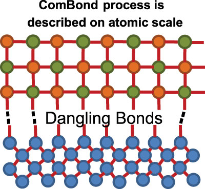
Figure 1: The ComBond process creates open bonds, which are also known as dangling bonds, on the semiconductor crystal surface. These bonds hold the key to wafer bonding of different materials covalently without an intermediate layer.
At EV Group of St. Florian, Austria, we have developed a technology called ComBond that is able to realize a covalent, oxide-free bond interface with ohmic behavior
Beside thermal expansion matching and the demand for low temperature, wafer size and die differences need to be handled effectively for heterogeneous integration. One downside of wafer-to-wafer bonding is that the pitch and placement of the die on each wafer must match up with one another "“ and even if this is done perfectly, every time, material is still wasted when one type of die is much smaller than the other. Wafer-level die transfer abolishes this geometry matching, thereby trimming material consumption while delivering high yield and throughput, by combining fast distribution of the dies and collective die transfer using wafer level fusion handling.
The remainder of this article covers in more detail the key aspects of all the wafer bonding processes outlined above. Read on to discover the techniques needed to realize a good bond, how to form an electrically conductive bond interface, and how die can be transferred at the wafer level.
One of the most common integration processes involves the forming of a silicon-on-insulator heterogeneous stack via fusion wafer bonding. Note, however, that this established, high-volume production process is not limited to this material combination, and can be used to form a wide variety of engineered substrates (see table 1 for a list of materials).
A key step in the bonding of compound semiconductor materials is the activation of the surface of the wafer by plasma treatment. Initial bonding takes place at room temperature, but strengthening of the bond interface requires a subsequent annealing step. Without activating the wafer surface, this takes place at around 900°C, a temperature not suitable for materials with different thermal expansion coefficients. Heterogeneous material integration falls into this category, so such high temperatures are ruled out, because the thermally induced stress would cause wafers to markedly bow, warp and even crack.
By avoiding any high temperature steps, our plasma-activated fusion wafer bonding process does not suffer a similar fate. With this approach, there is oxidation within the interface, and this allows high bond strengths with annealing at 300°C. At this much lower temperature, most material combinations do not get close to critical stress, and this allows almost any compound to be integrated on alternative substrates.
When performing this procedure, it is essential to use clean, flat wafers to realize a high-quality bond. If any particle inhibits the contact of the surfaces, voids will be present between them; and for fusion bonding to succeed, the roughness of the surface must be better than 1 nm.
The good news is that it is not that challenging to meet this pair of criteria. If wafers are too rough, they can be smoothed sufficiently with today's chemical mechanical planarization equipment. And if the interface is on SiO2, a known CMOS-compatible material, oxide deposition and chemical mechanical polishing can be performed on practically all wafers. The bonding interface places no restrictions on further downstream processing, because additional processing steps can take place in a high vacuum or at temperatures higher than the bonding or annealing temperature.
When the interface between the wafers has to be electrically conductive, surface oxides must be removed. This is not the only requirement for the surface treatment process, however: There should also be no damage added to the underlying bulk structure. If treatment were to introduce lattice point defects, such as interstitials and dislocations, this would provide traps for charge carriers that would impair final device performance.
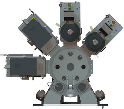
Figure 2: The EVG 580 ComBond vacuum cluster system
One option for producing oxide-free bond interfaces is to treat the wafers with hydrogen fluoride prior to bonding. However, hydrogen fluoride must be handled with great care, and disposing of the chemical is not trivial. What's more, a terminating hydrogen-layer forms on the wafer during its chemical bath, and removal of this monolayer requires a bake-out at 600 °C. Adding to the complexity of this approach, there is the need to avoid regrowth of surface oxides during handling and storage, both after the wet etch and during bake-out. Lastly, there is complexity associated with the chemical etching, which stems from different substrates and the integration with different compounds.
Our approach is much simpler to perform, using our ComBond technology to remove an undesired oxide layer with a dry process based on energized particles. It differs from the fusion bonding process that closes nanogaps via oxidation, with surface treatment taking place on an atomic scale to produce dangling bonds, the pre-requisite for the forming of covalent bonds at room temperature (see Figure 1).
The tool that we have built for this task is the ComBond Activation Module. It is ideal for wafer bonding, because it delivers effective oxide removal while simultaneously minimizing damage to the underlying substrate. Wafers are kept in a high-vacuum environment after surface treatment to prevent the re-oxidization of their first monolayer while undergoing further processing in the bonding cluster system (see Figure 2). With surface preparation only taking a few minutes for each wafer, re-oxidation can be prevented for several substrates and activation conditions.
All direct wafer-bonding processes require low surface roughness to ensure a uniform contact at the nano-scale. To demonstrate the high-quality of the surface treatment associated with our ComBond Activation Module, we have performed experiments on a range of materials. Scrutinizing surfaces with an atomic force microscope reveals that treatment with our tool does not roughen the surface, and might actually make it slightly smoother (see Figure 3). With a typical quadratic mean micro-roughness of less than 0.6 nm after oxide removal, these wafers exhibit excellent surface conditions for forming heterogeneous structures of the highest crystal quality.
Another virtue of our ComBond process is that it does not leave detectable residual oxides at the bond interface. Energy-dispersive X-ray spectroscopy performed on SEMI-standard silicon wafers that were bonded using the ComBond process failed to pick up any sign of oxygen at the bond interface.
Bonding of GaAs and InP wafers is a key step in the fabrication of very high efficiency solar cells with four or more junctions. We have studied this, covalently bonding GaAs to InP and inspecting the interface with a high-resolution tunneling electron microscope. Images indicate efficient removal of all the oxide and the creation of an incredibly thin amorphous layer "“ it has a thickness of less than 2 nm. This high-quality, electrically conductive interface is excellent at supporting vertical current flow, because it is not plagued with crystal distortions and trap states. The performance of multi-junction solar cells is enhanced by such a structure, which does not require a thick epitaxial buffer layer between the stacks and benefits from an optically transparent interface.
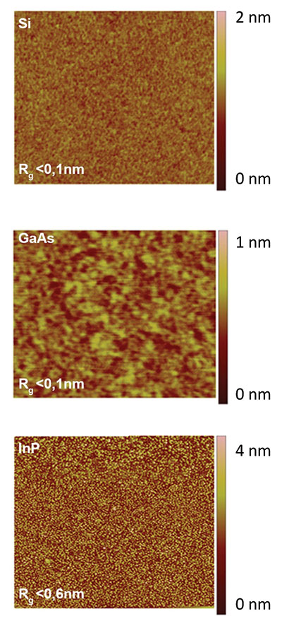
Figure 3: Atomic force microscopy images over a 2 mm by 2 mm area demonstrate that the ComBond Activation Module can produce surfaces after oxide removal that are smooth enough for bonding. To meet this requirement, the quadratic mean micro-roughness has to be significantly below 1 nm.
Multi-junction solar cells are not the only devices that benefit from a high-quality bond with a very thin amorphous layer "“ they aid any device that needs great electrical performance in the vertical direction. Power devices fall into this category: bonding SiC epistructures to polycrystalline SiC can slash wafer costs and spur the penetration of these devices into a broader range of applications; and a similar scenario could occur with vertical power devices made from GaN, which are very promising, due to high electron mobilities and breakthrough voltages.
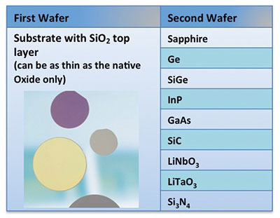
Table 1: Many compound semiconductor materials can be bonded by low-temperature plasma-activated wafer bonding and can be found in production today.
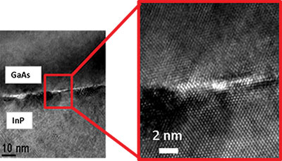
Figure 4: Transmission electron microscopy reveals that a GaAs/InP oxide-free, covalent-bonded interface has a thickness of less than 2 nm, and that the quality of the underlying crystal is not affected by the bonding process.
One downside of wafer-to-wafer bonding is that it can produce a significant loss of real estate. In some photonic applications, for example, there is a low fill factor for the target wafer that is equipped with electro-optical elements. On the other hand, the wafer sizes in CMOS technology are generally not the same as those used in the compound semiconductor industry.
It is important to also note that there several key advantages with wafer-to-wafer bonding, such as collective pre-processing of the dies and high bonding throughput, which are strengths that are impossible to provide with die-to-die bonding.
Fortunately, it is possible to combine the best of both worlds by employing fast distribution of known good die, using high-quality direct bonding at the wafer level. This approach reduces the sensitivity to thermally induced stress and decouples the yields to the two processes, so long as known good die are only placed on known good sites on the wafer. Tuning the bonding conditions is relatively easy, because collective bonding is possible at elevated temperatures, even in vacuum conditions.
For a wafer-level die transfer process to be successful, it is essential to apply an appropriate, uniform pressure to every single die. This is not easy, due to factors such as bow and warp of wafers, uneven substrates and differences in die height (see Figure 5). Introducing a compliant layer addresses all these challenges by enabling the application of similar force on different die, thus providing optimal transfer rates and high bonding yield.
Thanks to this process, heterogeneous integration can be scaled up to larger substrates and multiple functions can be added to the device wafer, even in volume production. This process "“ and that involving wafer-to-wafer bonding "“ will help to drive a new era for innovative device structures with novel functionalities and increased performance.
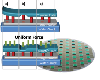
Figure 5: Several types of non-uniformities have to be considered for a high-yielding, wafer-level die transfer process: (a) bow or warpage, (b) unevenness of the substrates, (c) die height variation. These issues can be overcome by applying uniform force on the backside of the die using an efficient, compliant layer while bonding.
-
ComBond results were created with support from Dr. Dimroth at Fraunhofer ISE. EVG and his team are partnering for the development of highly efficient multi-junction solar cells.
T. Plach et. al. J. Appl. Phys. 113
094905 (2013)K. Hermansson et al. in Semiconductor Wafer Bonding: Science, Technology
and Applications IV/1998
A. Plößl et al. in Semiconductor Wafer Bonding: Science, Technology and Applications IV/1998
Flötgen et al. ECS Transactions 5 64 (2014)


