Meeting The Need For Low-Cost MOSFETs
On top of this, there are further prospects for electrical energy savings. One area is transportation, which is witnessing growth in sales of electric and hybrid electric vehicles and the construction of more electric aircraft; and there are also opportunities in the home, where greater electrical efficiency will help to drive the uptake of alternatives to fossil fuels for heating.
It is well known within the compound semiconductor community that replacing silicon devices with those made from wide bandgap materials can deliver a tremendous hike in the efficiency associated with power conditioning. That's partly because chips built from the likes of GaN and SiC have low resistive losses, which stems from their high critical electric fields; and it is also because these devices are capable of high switching speeds. An example of the superiority of wide bandgap devices over those made from silicon comes from the Arkansas-based firm APEI, which has developed an award-winning electric-vehicle battery charger based on SiC. This product highlights how wide bandgap devices can enable more efficient, smaller and cheaper systems, mostly in the consumer area using transistors capable of handling between 600 V and 1200 V.

Cost and performance
Today, the leading commercial wide bandgap technology for power electronics is based on the growth of epitaxial SiC on a native substrate − the 4H poly-type of SiC. Devices formed from this homo-epitaxial growth step can address a very wide range of applications up to 10 kV, but each area has very different requirements, in terms of performance, cost and the size of the market.
Although the sales of SiC devices are rising, silicon chips still dominate the power semiconductor market. One reason for this is that the SiC devices operating at 600 V and 1200 V, which could serve consumer applications, are seen as too expensive by many potential buyers, who are also concerned with the lack of compatible second sources. This is clearly not an issue when purchasing a silicon component.
There are two factors behind the relatively high cost of the 4H-SiC power device: 100 mm and 150 mm 4H-SiC substrates are very expensive, because growth of the crystal boules is a tremendously energy-intensive process; and device processing is costly and complex, due to the hexagonal form of SiC. The good news is that it doesn't have to be this way, because there is a low-cost alternative, the 3C poly-type of SiC. Reports of this form of SiC started emerging in the 1990s, with the Japanese firm Hoya leading the way as it strived for lower costs by developing a growth technique to create low-defect-density SiC-on-silicon substrates.
However, this is increasingly difficult with larger wafers, such as those with diameters of 100 mm or more. A high degree of tensile stress occurs at the interface between silicon and SiC, due to a combination of the crystal lattice mismatch between this pair of materials, and the higher coefficient of thermal expansion for SiC compared to silicon.
This issue did not stop researchers from Hoya demonstrating the promise of the SiC MOSFET, by fabricating devices with an excellent set of characteristics, which were formed via growth of 3C SiC on small silicon substrates. In this study, reported in 2002, engineers showed that this form of device can slash on-resistance under the gate, even compared to the best 4H-SiC MOSFETs of today.
Early progress by Hoya amounted to nothing, however. This Japanese firm was unable to produce larger wafers, and this lack of success led to closure of activity in this area. But our team at Anvil Semiconductors − a start-up based in the UK cities of Coventry and Cambridge − has shown that there is a great future for this class of device, because it is possible to address the stress at the interface between silicon and the 3C poly-type of SiC.

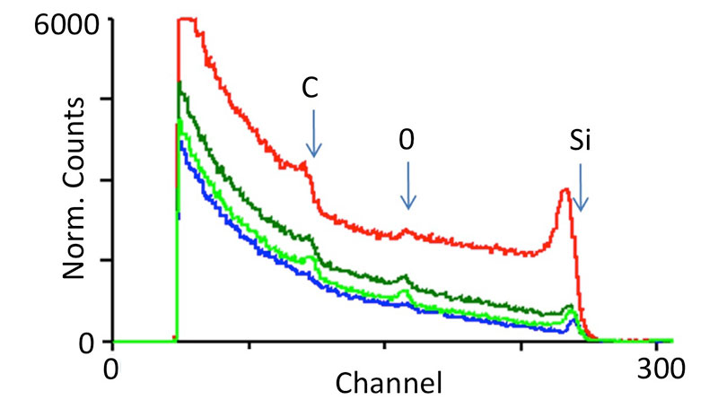
Rutherford Backscattering Spectroscopy is a method of assessing the defect density of a crystal by applying a beam of high-energy ions and measuring the energy of those ions which are reflected (Backscattered) by the crystal. The more perfect a crystal is, the more it absorbs the ions − defects in the crystal reflect the incident ions. In this case the Blue curve shows the backscattering from our native 3C-SiC crystal, which is dramatically increased by the defects introduced by Al ion implantation (Red curve). However after annealing at 1250°C (dark Green) or 1350°C (light Green) the RBS data suggests the defectivity has returned to the unimplanted state. This simple process is totally ineffective in 4H-SiC and demonstrates a major advantage of 3C-SiC over 4H-SiC.
To unlock the commercial potential of this class of MOSFET, we have recently installed a production process for 100 mm wafers at Norstel AB. A key part of this process involves exploiting the normal scribe lane pattern that can divide active die on a wafer. Taking this approach minimises the dimensions across which stress is developed, and gives rise to an active stress relief structure.
This patented technology involves the forming of a SiO2 grid in the scribe lanes prior to epitaxial growth. Any SiC that is then grown in these regions takes on the polycrystalline form of SiC. Typical grid pitches are 2.5 mm and 5 mm, and thanks to the high current densities that can be realised in SiC, a 10 A vertical device can be constructed from a 2.5 mm die. Electrical resistance at the Si/SiC interface in these devices is indiscernible, due to the combination of dopant up-diffusion from the n+silicon substrate and an added dopant at the interface; and growth of layers with thicknesses up to 12 mm are more than adequate for a 1200 V transistor. Note that one of the great merits of this stress relief technique is that it is, by design, independent of wafer diameter. This will allow us to scale our process to larger wafers, which could be produced on multi-wafer Aixtron reactors.
Bow profiles acquired at the end of our epitaxy process reveal that the central area of the wafer, which is defined as that spanning the range ±50 mm high, occupies more than 70 percent of the total wafer area. We have scrutinised these layers by a variety of common characterisation techniques, including AFM, TEM, SEM, XRD and cathodoluminescence, and shown that their quality is at least as high as that produced by Hoya's engineers. That's partly because some of the crystal defects seen by the team from Japan are avoided by working with a (100) off-axis silicon substrate that drives a step-flow epitaxial growth process.
By employing all this know-how, we can produce SiC-on-silicon wafers with very low defect densities that can be processed into devices capable of handling current densities of at least 500A/cm2. Although the growth process leads to steps that are typically 8 nm in height, chemical mechanical polishing can trim surface roughness to below 0.5 nm
Similar to silicon
When it comes to post-growth processing, 3C-SiC has many advantages over the 4H poly-type. Switching from a hexagonal to a cubic crystal structure simplifies the introduction of dopants by ion implantation, because damage recovery of SiC is far easier to perform. What's more, implantation can be carried out at room temperature, avoiding the need for specialist high-temperature implant equipment and complex hard mask processing. Meanwhile, damage recovery only requires annealing at 1350°C, which in turn preserves the material surface.
It is also easier to put the finishing touches to SiC MOSFETs formed from the 3C poly-type, than it is to those based on the 4H form. Gate oxides grown on 3C-SiC do not suffer from an interface state problem that adds to the on-resistance of 4H-SiC transistors; and 3C-SiC is much more reactive to metals for the ohmic contact, so it is not necessary to use the extreme metal annealing temperatures required for 4H-SiC. The upshot of these advantages is that a 3C-SiC-on-silicon MOSFET process flow is very similar to that of a silicon DMOS device, making it possible to manufacture this wide bandgap transistor on a standard silicon MOSFET line with the sole addition of a high-temperature annealing furnace.
If devices are made in this manner in high volumes, the cost for making a 650 V, 3C-SiC-on-silicon DMOS power transistor should be very similar to that for producing a superjunction silicon MOSFET.
The 3C form of SiC also trumps its 4H cousin when it comes to packaging and hybrid assembly. It is tricky to interface the back of a 4H-SiC die with a package or hybrid board because a typical back metallisation is a type of nickel silicide, rather than mainstream assembly metallurgy. Making matters worse, this back contact demands high-temperature processing, so it must be formed at the appropriate point during front-of-wafer processing. In sharp contrast, the back of our wafers are made from silicon, so we can use any conventional die attach technique. This enables us to thin a 100 mm wafer to 100 mm, and then employ a standard gold eutectic process.
Our prototype Schottky barrier diodes exhibit excellent material quality and verify the technology and processing steps. These devices produce ideal characteristics, are free from SiC-silicon interface effects and have good crystal quality, resulting in extremely high yield.
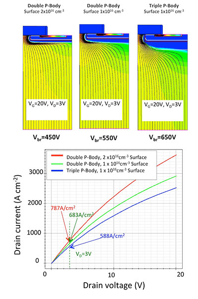
The next steps for us include realising further process improvements, leading to the fabrication of Schottky barrier diodes for sampling. In addition, we aim to qualify high-quality MOS gate oxides and develop the MOSFET process and device design. The latter activity involves extensive device simulation using the best numerical models (an example is shown in Figure 1, which suggests that superior channel mobility in 3C-SiC results in roughly half the on-resistance of a 4H-SiC equivalent).

The primary opportunity for 3C-SiC devices in the power semiconductor market
As stated before, we are targeting the 650 V to 1200 V device sector with designs that should be very cost competitive. Such products would appear to be competing with those that are emerging sporting another promising technology, GaN-on-silicon. There is an abundance of MOCVD reactors capable of GaN epitaxy, and there is a considerable worldwide development effort underway in GaN HEMTs.
While a complete discussion of the merits of SiC-on-silicon over GaN-on-silicon is outside the scope of this article, it is worth pointing out some of the shortcomings of the latter technology. First, some very advanced technology steps have been required to turn the normally on HEMT into a MOS-like enhancement mode GaN device. However, have these new elements that have been introduced to switch off the HEMT created a truly a normally off device that can be applied in safety critical systems?
Adding to the concerns, it seems that the GaN HEMT will remain a lateral device for the foreseeable future, albeit perhaps one featuring a through-substrate via to bring the drain to the back of the device. This architecture leads to a much lower power density than a vertical device, with typical published layouts essentially incompatible with conventional packages or hybrids. In short, applying this very interesting technology in the power arena is going to be far from trivial.

Figure 1: The fundamental compromise in MOSFET design is between on-state conduction and off-state blocking voltage. The on-state conduction is essentially set by the JFET structure formed by the edge of the P-Body and the n-epitaxy, while the blocking voltage is determined by the electric field intensification at that same edge of the P-Body. As these two effects operate against each other a compromise is required. This simulation, optimised for a 650V device, shows three different P-Body structures and a current carrying capability of the device of 588 A/cm-2. This demonstrates the high current capability of this technology, for example a 10A MOSFET would only require a die of say 4 mm2, taking account of the additional area for contacts etc.
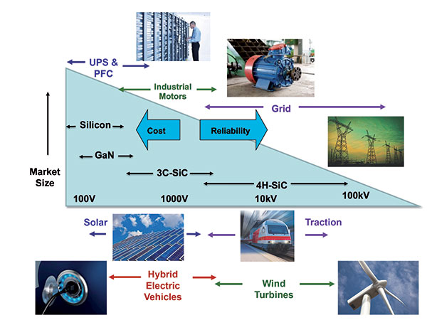
Based on this reasoning, we see the future market segmentation of wide bandgap devices like this: GaN-on-silicon will certainly find applications in the 100 V to roughly 400 V segment, 3C-SiC-on-silicon should occupy the 600 V to 1200 V ground, and above 1200 V is the territory of 4H-SiC. To convince the power electronics sector of this, we plan to supply prototype Schottky barrier diodes to selected customers in the current quarter, and follow this up with prototype MOSFETs in the third quarter of this year.
Further reading
Wan et al, IEEE Electron Device Letters 23 482 August 2002.


