
Will III-Vs Make An Impact In Next-Generation CMOS?

Rewind the clocks a few years in the silicon industry, and it would only require a simple story to outline the path of progress associated with this technology. Back then, engineers would improve circuit performance while cutting costs by taking the existing transistor and trimming its dimensions.
Recently, however, complexity has dogged the story of silicon. There has been the introduction of hafnium dioxide, so that the gate dielectric doesn't leak electrons. And this device has had to rise out of the plane of the substrate, so that it can maintain its traditional levels of improvement with each generation of scaling.
Even greater changes are on the cards in the next decade or so, with the silicon in the channel of the transistor expected to make way for higher mobility materials that will enable high levels of performance at lower operating voltages. InGaAs is a strong contender for taking over the nFET, while germanium is tipped for making an entry into tomorrow's pFETs.
Both of these materials were discussed at the recent International Electron Devices Meeting in San Francisco on 15-17 December, 2014, where several groups reported results of experimental work and calculations relating to post-silicon transistors. In this latest chapter of the silicon story, conflicting accounts were presented of the promise of these alternative materials for making an impact in tomorrow's silicon foundries.
Go with germanium?
One paper questioning the potential of InGaAs for improving n-type finFETs came from a team from Samsung Semiconductor. They have calculated that this ternary would not deliver the necessary improvement over silicon, in terms of carrier transport properties, because it would not produce the expected ballistic performance in a device with dimensions suitable for a next generation transistor.
"I was somewhat surprised [by this result]," revealed Seonghoon Jin during an interview with Compound Semiconductor. "Regarding the reasons, both the low density-of-states and strong surface-roughness scattering are important factors."
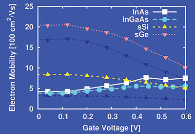
Figure 1. Calculations by a team from Samsung suggest that channels made from strained germanium can offer a higher mobility than those formed from InGaAs. Note that the darker lines with triangles are for unstrained channels of germanium and silicon.
A key aspect of this work is that both the coupled multi-subband Boltzmann transport equation and the drift-diffusion equation are solved self-consistently to evaluate finFET performance with new channel materials. "I think that the modeling methodology is state of the art," argues Jin, who included in the calculation some features that are particularly important to III-V channel finFETs, such as surface roughness scattering, a density-gradient model, and band-to-band tunnelling.
According to Jin, one strength of the team's calculations is that by solving the multi-subband Boltzmann transport equation in the channel, the effects of band structure, quantization and quasi-ballistic transport are accounted for. The distributed contact resistance and non-uniform current path are also considered, thanks to the solving of the drift-diffusion equation in the source and drain regions.
The team calculated the performance of a device that is a simplified version of the future node finFET and has a fin width of 6 nm. Calculations considered four channel materials "“ InAs, In0.53Ga0.47As, silicon and germanium "“ and for the latter two materials, the impact of tensile stress was included (see Figure 1).
Self-consistent simulations suggest that a silicon channel provides the largest inversion charge, but the lowest injection velocity; an InAs channel offers the highest injection velocity, but the lowest inversion charge; and germanium delivers the highest mobility, which is realised with a reasonable carrier density.
Given these attributes, it is not surprising that the calculations suggest that a strained germanium channel delivers the highest on-current. However, when the team included a more realistic contact resistance in their model, drain current fell sharply, so it is imperative that this resistance must fall if n-type strained germanium is to become an attractive option for tomorrow's nFETs. If that does not happen, strained silicon can deliver better performance.
Or are III-Vs better?
A more positive view on the role of InGaAs in future ICs came from a paper presented by Enrico Caruso and colleagues from the University of Udine, Italy. Caruso told Compound Semiconductor that at a supply voltage of 0.5 V, the team's calculations suggest that on-current for InGaAs exceeds that for silicon by about 30 percent. "It must be stressed that III-V materials have a switching time smaller than silicon, so even if the current is the same, it is possible to increase the performance anyway."
Caruso believes that one of the most important aspects of the team's work is that it takes into account most of the physical effects necessary for the characterization of MOSFETs with a III-V channel. "In particular, it accounts for far-from-equilibrium carrier transport in the channel, size and bias induced quantization, and the effect of interface traps on the transport."
There are weaknesses of the model, however: It is semi-classical, so it does not include quantum effects in the transport direction, such as band-to-band tunneling and source-to-drain tunneling. "Simulations in this work do not consider series resistance, and thus our results should be regarded as an upper limit for device performance," argues Caruso. He also points out that although the short-device simulations are far from equilibrium, trap states along the channel are populated using an equilibrium Fermi-Dirac distribution. "We think that the interplay between strain and interface traps should be further verified with more accurate atomistic simulators."
The team from Udine has modeled the performance of strained and unstrained InGaAs and GaSb channels with an 11.7 nm gate, a length expected to be introduced in foundries in 2020 according to the International Technology Roadmap for Semiconductors. Using an appropriate well thickness of 6 nm, the theorists found that In0.53Ga0.47As channels can outperform those made from strained silicon, in terms of drain current, for gate-source voltages up to about
0.55 V "“ beyond that, this III-V suffers from a density-of-states bottleneck. Meanwhile, GaSb fails to deliver any improvement in on-current compared to InGaAs, even in the ballistic limit. However, this antimonide could be competitive at a well thickness of 3 nm, thanks to quantization effects that produce changes in carrier mass.
One option for increasing the electron mobility of InGaAs is to introduce strain into this material. However, calculations by Caruso and co-workers show that this only delivers limited benefits up to a strain of 0.5 percent, due to Fermi-level pinning.
A consequence of the low effective mass of electrons in In0.53Ga0.47As is that source-to-drain direct tunneling is more prevalent in these MOSFETs than those made from silicon. "It is expected that source-to-drain direct tunneling can be a major obstacle in downscaling III"“V MOSFETs into channel lengths below 20 nm, but our model does not capture this effect and for this reason it is difficult to do some prevision for the design," admits Caruso. To address this weakness, the team is coordinating efforts in a European project involving eight partners, including IBM and Synopsys, that will compare the results of Monte-Carlo and non-equilibrium Green's function models.
Encouraging signs for InGaAs
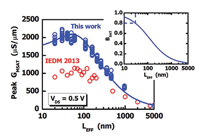
Another paper offering a more positive view of InGaAs FETs came from a team from the IBM Research Division based at the TJ Watson Research Centre in Yorktown Heights, NY. Corresponding author of the paper, Yanning Sun, toldCompound Semiconductor that she believes that one of the most important aspects of the team's work is that it demonstrates self-aligned and scaled III-V devices using device structures and process flows that are CMOS-compatible and manufacturable. Compared to other devices reported in the literature that utilise the least damaging process conditions, but are not CMOS-compatible, Sun claims that the team's devices have performances among the best In0.53Ga0.47As FETs (see Figure 2).
An important, recent finding by the IBM team "“ based on investigating the impact of barrier and channel doping "“ is that as gate lengths are reduced below 40 nm, the benefits of a mobility of more than 500 cm2 V-1 s-1 get smaller and smaller (see Figure 3). "At the 10 nm node, devices are expected to operate in the quasi-ballistic mode, and we believe that a mobility higher than 1200 cm2 V-1 s-1 does not add a significant contribution to device performance," says Sun.
The team is yet to make devices as small as this, but it has produced In0.53Ga0.47As channel MOSFETs on InP substrates with effective gate lengths as short as 20 nm. The performance of these devices is better than those it reported at IEDM 2013: Transconductance has doubled, primarily due to the combination of a halving of parasitic resistance, a 50 percent increase in high-field mobility and a 25 percent gain in inversion capacitance. MOSFETs with an effective gate length of 30 nm can produce a peak saturation transconductance in excess of 2200 mS/mm, while sporting an external resistance of just 270 Ω mm, and those with an effective length below 30 nm can operate within 20 percent of the ballistic limit.
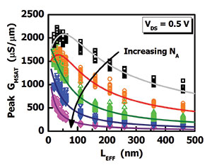
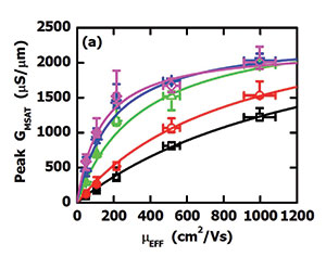
Figure 3. The plot on the left shows that the peak saturation transconductance, GMSAT, falls with increasing channel/barrier doping for MOSFETs with an effective channel length of 20 nm. The plot on the right shows the relationship between peak transconductance and mobility for effective gate lengths ranging from 30 nm to 260 nm.
It is possible that at some point the team may wish to switch from making planar devices to finFETs. If they decide to do this, the transition should not prove too taxing, because many of the process modules are capable of forming non-planar devices, including the tools used for active-area definition, gate patterning, spacer formation, extension implantation and selective source-drain regrowth. "The detailed conditions of some modules certainly need some adjustments, such as etch time and implantation angle, due to the device topography," says Sun.
The IBM team's plan for the future is to improve device performance through a combination of further scaling, greater mitigation of short-channel effects and a cutting of parasitics.
Although the last five years have witnessed substantial improvements in the drive current and transconductance of III-V MOSFETs, these devices have been plagued with high leakage currents. This is a major issue for the deployment of this class of transistor in battery-powered applications, because the large losses in standby-mode would have to be combatted with unacceptably short intervals between charging. At the recent IEDM meeting, Cheng-Ying Huang and co-workers from the University of California, Santa Barbara (UCSB), unveiled a new design of III-V MOSFET that slashes the leakage current (see Figure 4).
Although the last five years have witnessed substantial improvements in the drive current and transconductance of III-V MOSFETs, these devices have been plagued with high leakage currents. This is a major issue for the deployment of this class of transistor in battery-powered applications, because the large losses in standby-mode would have to be combatted with unacceptably short intervals between charging.
"High mobility channels usually result in high leakage due to band-to band tunnelling near the drain, which will eventually limit device scalability," explains Huang. "We addressed how to control the leakage current of the III-V MOSFET at VLSI relevant dimensions, eliminated band-to-band tunnelling leakage using a wide bandgap source and drain spacer, and made III-V MOSFETs feasible for low-power logic applications."
The devices made by the UCSB team are planar MOSFETs with a 4.5 nm-thick InGaAs channel and a doping-graded InP spacer that can realise an off-current of just 60 pA/mm.
Huang explains that these "ultra-thin channel devices" are not optimised for low-power because the thin channel has both its pros and cons: It improves electrostatics, but at the expense of inferior electron transport and on-state current.
"For the 7 nm node, we need finFET structures to improve transistor electrostatics," argues Huang. According to him, for low-power and ultra-low-power logic, leakage must not exceed 30 pA/mm and 15 pA/mm, respectively, and in this regime the gate overdrive voltage is mainly on the sub-threshold region. "Improving transistor electrostatics using finFET structures will improve sub-threshold swing, thereby increasing the on-current at a fixed off-current."
To make the MOSFET process compatible with high-volume manufacturing requires a change of substrate and device miniaturisation. "Although our devices are not on silicon and contacts not fully scaled, our process flow uses gate-last and source/drain regrowth processes," says Huang, who points out that for the last few years, gate-last and source/drain regrowth processes have already been used in silicon CMOS processes.
One of the next goals for the team is to fabricate III-V MOSFETs on silicon substrates. In addition, the West-coast researchers are trying to reduce the off-current of the MOSFETs to 10-30 pA/mm, optimise the source and drain spacers, and to increase the on-state current.
Nanowire tunnel FETs
Another form of device that is already capable of exhibiting low leakage currents − and promises to do even better in this regard − is the InGaAs/InAs single nanowire vertical tunnel FET. This class of transistor, which has been fabricated by Xin Zhao and colleagues from MIT, has been formed using a novel III-V dry etch process. At an operating voltage of 0.3 V it has an on-current of 0.27 mA/mm at a fixed off-current of 100 pA/mm.
These results highlight the protential of the tunnel FET, which is to operate at a lower voltage than a MOSFET by realising a sub-threshold swing steeper than the thermal limit of 60 mV/decade.
Zhao says that the most important finding detailed in the MIT paper is the identification of a possible leakage mechanism for the tunnel FETs: tunnel-assisted generation that precludes the possibility of achieving a sub-thermal sub-threshold swing.
"This mechanism involves tunneling of electrons into the trap states and subsequent thermal generation of carriers into the conduction band," says Zhao, who argues that it is this mechanism that might explain the temperature-dependence of the sub-threshold current in many tunnel FETs. This leakage results from trap states, particularly at the interface, and it prevents the promise of a sub-thermal sub-threshold swing.
To form their devices, the engineers use reactive ion etching, a technique used in the optics industry to form micron-scale structures with high aspect ratios. "To our best knowledge, our reactive ion etching technology presents the first demonstration of sub-20 nm features with vertical sidewalls in indium-based heterostructures," says Zhao.
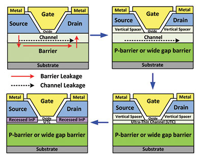
Figure 4. A team from the University of California, Santa Barbara, have developed a design of III-V MOSFET that realises a far lower leakage current, and is thus suitable for low-power applications.
Tunnel FETs are a relatively new technology, so there are yet to be any well-established projections for technology nodes for this device. However, Zhao says that he and his colleagues will need to make further improvements in their reactive ion technology, in terms of reduced footing and trenching, if it is to become applicable to the production of devices at the sub-10 nm node. The promise of this device and those of other III-V FETs described in experimental papers at IEDM bodes well for the future of compound semiconductor technologies for future ICs, while the work of some other groups, in particular the calculations presented by Samsung, suggests otherwise.
"The jury is up whether III-V FETs will find themselves in future chips with sub- 10 nm technology nodes," says Zhao, who points out that there are some major challenges that must be overcome, such as the construction of prototype devices with appropriate dimensions. "Theoretical papers have mixed predictions and further efforts of calibration against experiments are needed."
Huang agrees with Zhao, saying that it's not clear whether III-Vs will make an impact. He points out that for this to happen, these new materials will have to deliver a substantial performance advantage, in order to justify the expense of developing a production technology. His view, which is surely shared by many others, is that we will all just have to wait and see how the competing technologies will evolve over the next couple of years.


