
The Resurgence Of Electron Beam Evaporation

After decades of playing second fiddle to sputtering in the silicon industry, electron beam evaporation now dominates in the compound semiconductor industry, thanks to its inherent advantage in the lift-off process
Everybody likes a comeback story. It's uplifting to see an underdog claw out of the trenches, grow in strength, and eventually emerge victorious.
Head to the cinema, and you'll see plenty of films with this storyline. But the great comeback is not limited to the silver screen "“ sometimes it happens in real life, right within our own industry.
Take, for example, the fibre optic sector. Back in the late 1990s, stock prices in III-V companies operating in this realm reached astronomical valuation, as telecom firms from all over the world started to expand their network capacity to meet a projected surge in traffic. But that super-high level of growth failed to materialize, contributing instead to the "˜dot.com' bust at the turn of the millennium. Fast forward to today, however, and business is booming again for the providers of optical components for communications, thanks to growing demand for more and faster data.
This is by no means the only comeback kid in our community. There is also the electron-beam evaporation. Along with sputtering, it dominated the semiconductor industry in the 1960s and early 1970s, before the growth of microelectronics led to greater sales for sputtering tools for ever larger silicon wafers. Only in recent times has the situation reversed, with the electron-beam evaporator resuming its ascendancy, thanks to compound semiconductors capturing ever higher revenue from the soaring shipments of mobile devices. These devices feature compound semiconductor chips manufactured on production lines utilizing electron beam evaporators, which have superior uniformity and a lower cost-of-ownership than the other three established thin film deposition techniques (see panel "˜Four options for metallization' for details of all techniques).
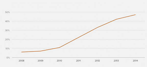
Figure 1: The percentage share of mobile device in the overall consumer electronics industry.
Of these four vacuum-based techniques for metal deposition, those that are best at serving the semiconductor industry are electron-beam evaporation and sputtering. They both have a long history, having been developed in the mid-nineteenth century. The roots of sputtering are found in the efforts of the Welshman Sir William Grove, who noticed deposits in the anode of a gaseous discharge, which was removed following a reversal of the polarity of the electrodes. Meanwhile, the beginnings of electron-beam evaporation can be seen in the work of English physicist Michael Faraday, who used a voltaic battery to deposit gold on a glass substrate, albeit with poor adhesion.
About a hundred years later, requirements of microelectronics drove the development of electron-beam systems for metallization. One of the pioneers was Temescal, and we remain a leading player in this field, owned by Ferrotec (USA) Corporation. We hold the original patent for 180° beam-deflection sources − that were widely used in early generations of electron-beam systems − and also 90° sources. Both approaches had a flaw, with wafers damaged by X-rays emitted with the beams. To address this, in 1972 we developed the patented 270°-deflection electron-beam source. This is now commercially adopted worldwide for electron-beam evaporation. However, at the time of its launch, sputtering was already viewed as the superior deposition process.
We moved with the times, and through Airco-Temescal we patented and developed apparatus using magnetron sputtering (see Figure 2). This technology held the upper hand due to its lower operating voltage and its simplicity in the use of masks for ensuring uniform film deposition. Note that in electron-beam systems, the multiple masks employed to achieve the best uniformity for each layer of a given metal stack are not stationary and generate particles during movement.
Sputtering also brought benefits in terms of versatility, as it can deposit complex films, such as refractory metal composites and metal nitrides. What's more, it can handle wafers with large diameters, including those up to 450 mm, and this gives it overwhelming advantages for the metallization of silicon devices.
However, electron-beam evaporation has never gone away, because it also has virtues. This deposition technique is isotropic and can limit unwanted sidewall coverage during the lift-off process. This step is widely used for producing compound semiconductor chips, and is generally preferred to the lift-off of a sputtered film with the assistance of CO2 gas injection to break down the unavoidable sidewall coverage from sputtering. Electron-beam evaporation also offers significantly superior cost-of-ownership from its high-volume batch process, plus higher yield, thanks to elimination of the unwanted metal sidewall in the lift-off process.
It is these attributes that are behind the resurgence of the electron-beam evaporator, which has grown in sales as the manufacture of compound semiconductor chips has soared throughout the last decade. A hike in smartphone sales has been a key driver. Sales took off in 2007, with compound semiconductor fabs throughout the world experiencing a vast increase in demand for power amplifiers, filters and switches used in smart phones. Up until then, only the Blackberry made by Research In Motion offered enterprise email access through secure servers. It took 11 years for this company to gain 41 million subscribers, but it didn't stay at the top for long "“ Apple's iPhone took the market by storm, with annual sales hitting 40 million in just 11 quarters, due to a design delivering a previously unimagined level of productivity improvement. Google subsequently upped the ante, offering a free and open operating system for smart phones. This rapidly propelled Google's Android OS to leading position in 2010 (see Figure 3).
Around this time, the LED market underwent a revolution. It evolved from just illuminating the screens and keypads in handsets to LCD backlighting and then general lighting. China has played a major role in the development of this industry, helping to fund the founding of its domestic LED chipmakers, and this has contributed to the rocketing demand for electron-beam evaporation equipment.
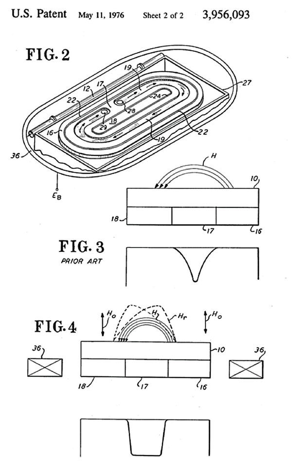
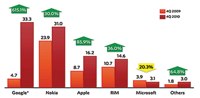
Figure 3: The ascension of the Google Android OS for smart phone.
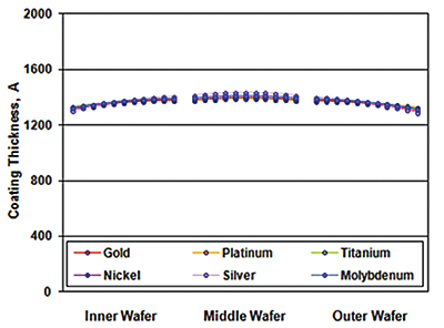
Figure 4: The thickness variation of common metals in a HULA evaporator is very small, even without any uniformity mask.
Innovations in system design
As stated previously, it is not easy to always realize a high level of thickness uniformity with electron-beam evaporation. This deposition technique can produce excellent thickness uniformity by positioning a single wafer optimally. But typically a multi-material-layer metal stack is deposited in a single-axis-of-rotation multi-wafer batch system; a high level of thickness uniformity could only be achieved with multiple masks, many of which must be movable. That is undesirable, because moving masks may generate particles.
Uniformity masking is optional, however, with our patented High Uniformity Liftoff Assembly (HULA) technology that generates no particles, thanks to a contactless magnetic drive. Highly uniform films result, due to the planetary configuration of the multi-dome assembly that provides time averaging on wafer residence across the product chamber. With this tool, nearly every evaporant can be deposited with a uniformity of less than 3 percent (see Figure 4), which is adequate for many applications − but even higher uniformities can be reached by adding a small mask. This inherently more uniform HULA evaporation also gives rise to saving in the purchasing cost of evaporants, because the material collection efficiency on wafers is 43 percent higher than that of traditional single-axis wafer carriers.
Efforts to improve uniformity are also aided by our extensive vapour cloud modelling. This has resulted in a rapid advance in the technology of the uniformity mask, cutting the time it takes to generate an optimized mask for any metal stack. This breakthrough, together with the combination of improved magnetic assembly for the electron-beam source, faster pumping speed and the isolation of the product chamber from the source chamber via load locking, trims the cost-of ownership of our electron-beam system while increasing process stability and system reliability.
The next frontier for electron-beam evaporation is to drive down particle generation during evaporation. One of the causes is the spitting of gold, which is a function of the contamination introduced by adjacent sources in a conventional multi-pocket electron-gun or during the refinement process of gold. Temescal's patented poptop technology virtually eliminates any cross contamination from adjacent pockets thus maintaining the purity of gold (see Figure 5). The issue of contamination can also be mitigated by using Materion's low-carbon gold. Moving mechanisms also generate particulates, which is why we have developed the contactless, magnetically driven wafer holder assembly (see Figure 6).

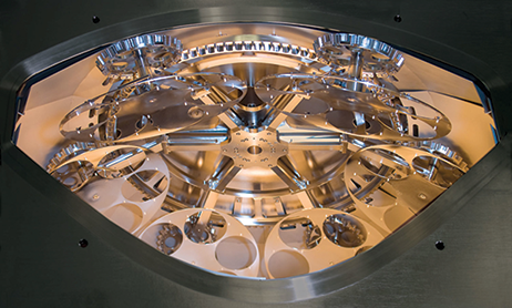
Figure 5: The thickness variation of common metals in a HULA evaporator is very small, even without any uniformity mask.
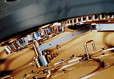
Figure 6: The HULA wafer holder assembly cuts particle generation, thanks to a magnetic drive system.
Another area where we have devoted much effort is in the mapping of the magnetic flux around the electron gun to produce an optimal beam shape. This has led to refinements in our capturing of secondary electrons, by upgrading the magnet material and magnetic assembly. By employing our patented placement of the magnet at the back of the electron-gun, we minimize the impact of secondary electrons on the photoresist.
Emerging trends in copper, eutectic and ultra-thin films
One way to cut chip costs in compound semiconductor fabs is to switch from precious metals, such as gold and platinum, to copper. This appears to be a good strategy "“ in a paper by Kezai Cheng from Skyworks, given at the 2009
CS Mantech conference, he noted that in addition to lower wafer cost, evaporated copper offers other technical advantages, such as lower resistivity and a reduced likelihood of spitting at high deposition rates.
Although the traditional method for depositing copper is electroplating, Cheng formed films with our electron-beam evaporator. In his paper, he offered three reasons for an evaporation and
lift-off process: the existing tool set used for depositing the ohmic and the gate metal can be set up to run copper; the evaporated first interconnect layer of copper does not require additional wet steps of seed layer removal, whether it is de-plate or chemical etch; and copper can be evaporated at high rates with minimal risk of spitting. He concluded that throughput for the copper process using electron beam evaporation would be similar or higher than that by electroplating. Furthermore, for any given tool set, throughput with copper would be higher than that with gold.
Other groups have also succeeded in developing processes for copper interconnects and electrodes by electron-beam evaporation. Research teams in Taiwan reported the forming of a 2 mm-thick copper interconnect for power HEMTs, and demonstrated a Pd/Ge/Au ohmic contact and a Ti/Pt/Cu seed layer of interconnect for a InGaP/GaAs HBT, using electron-beam evaporation. Another class of material used for both silicon and compound semiconductor manufacturing is the eutectic film. It is made from a homogeneous solid mix of atomic and/or chemical species that form a joint superlattice. Eutectics are employed in wire bonding, wafer bonding for die stacking, and hermetic encapsulation for wafer-level packaging.
Ensuring a change from solid to liquid during the bonding process demands a specific compositional ratio of the constituent materials, with optimal soldering only occurring within a +/- 0.5 percent compositional window. Straying outside of this range is detrimental: Engineers from Materion have shown that a 0.75 percent shift in composition in a eutectic with 80 percent gold and 20 percent tin increases the melting temperature by 30 °C and degrades bonding quality.
If a eutectic film is formed by a magnetron sputtering system, its composition is governed by the deposition power and chamber pressure. This places stringent demands on the control of both the processing parameters and the composition of the sputtering target.
It is a different story with electron-beam evaporation. In this case, it is possible to evaporate each metal component of the eutectic film on the wafer sequentially, before they inter-diffuse naturally, without any annealing, to form the desired eutectic film. Since the thickness of each film can be precisely controlled with ease, control of the composition ratio is much tighter than that achieved by sputtering − HULA evaporators are capable of controlling the eutectic composition to +/- 0.2 percent (see Figure 7).
This type of evaporator is also inherently suited to the deposition of uniform, ultra-thin films. These are 50 à… or less films − making thickness control very challenging via sputtering − and they have been grown by our customers in the mobile device, hard disk drive, LED and power electronics industries (see Figure 8).
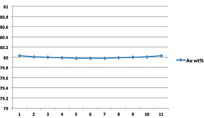
Figure 7: Control of AuSn eutectic composition in HULA across wafer without using any uniformity mask.
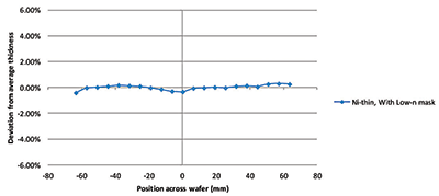
Figure 8: An illustration on the thickness uniformity of ultra-thin films evaporated from a HULA evaporator, with and without a mask.
Capability of ultra-thin film growth is just one of the many reasons that we have highlighted for the resurgence of the electron-beam evaporator, which has an inherent advantage in the lift-off process widely used in the manufacture of compound semiconductor chips. The cost-of-ownership of evaporators can be very low, due to parallel processing of many wafers, such as 42 6-inch wafers. This should help to trim the cost of connected devices which, according to Strategy Analytics (see Figure 9), could reach 33 billion units worldwide by 2020. To support the compound semiconductor industry for the competition in this booming market, we are addressing the new processing advances in copper, eutectic and ultra thin film deposition.
- The author would like to thank Gregg Wallace, Kuohsiung Li and Lyell Warren for their inputs on the development of this article.
Metallisation is a key process in the manufacture of compound semiconductor devices. It is used to form electrodes and interconnects, with up to 40 percent of the entire wafer covered by metals. The most common of these that are applied to compound semiconductor chips are gold, titanium, platinum, nickel, germanium and aluminium, and they may be added using one of four common techniques:
Etching. In this subtractive process, physical vapour deposition, in the form of electron-beam evaporation or sputtering, adds a metal or oxide film on to the substrate. This is patterned with a resist, before the unprotected material is removed with a dry or wet etch process.
Electroplating. A metal seed layer is first deposited via sputtering or electron-beam evaporation. After a photoresist is applied and developed, the wafer is electroplated before a chemical washing step removes the photoresist and the seed layer beneath it.
Damascene: In this additive process, patterns are etched into the dielectric substrate before a conductive metal is deposited onto the entire wafer. Chemical mechanical planarization removes any excess metal to leave inlaid metal in place on the wafer.
Lift-Off:Another additive process, this time involving the development of a sacrificial photoresist layer using a patterned mask. Evaporation or sputtering then adds a blanket coating of metal, before a lift-off wash removes material deposited on the photoresist. Metal that has been in direct contact with the wafer remains.


