Targeting A Terahertz Transistor
A spectral famine is looming at radio frequencies, due to exponential growth of wireless data transfer. However, at other slices of the electromagnetic spectrum an opportunity to feast is on offer, thanks to frequency bands that are largely untapped.
Terahertz frequencies represent one such opportunity, with progress pegged back by the difficulties of building sources operating in this domain. But if these challenges could be overcome, it would be great news for mankind. It could open the door to ultra-high speed circuits used for information and communication systems, including those operating wirelessly, as well as terahertz imaging systems and spectroscopy detection.
In recent times, researchers have taken two different tacks to reach the terahertz domain: going down in frequency for optical devices, and increasing the frequency for electronic devices. The optical approach involves semiconductor intersub-band sources, such as quantum cascade lasers (QCLs), while the leading electronic devices have been complex systems "“ for example, a Schottky contact diode with an integrated oscillator that may provide terahertz detection. All devices are based on electron-phonon interactions, with today's QCLs working mostly at low temperatures, limiting their deployment.
What's needed is a new approach that avoids temperature-related issues and is based solely on electron drift in high-power electronic devices. This is a goal that we are pursuing at the Slovak Academy of Sciences, where we have made some promising progress towards a novel HEMT featuring an InN channel.
A fundamental question that we have faced in our quest for higher speeds is this: What material shall I build my device from? One candidate is graphene, a material that has attracted a great deal of hype, in some cases for good reason. This atomic sheet of hexagonal carbon is blessed with an extremely high mobility, but it is a metallic system, so graphene transistors cannot be pinched off, limiting their use.
Transistors made from III-V channels don't suffer the same fate, which is why we have chosen them to pursue a terahertz transistor.
There are several options in this regard, and we have decided to focus our attention on III-N HEMTs, because they are known to have a higher critical breakdown field, greater robustness, higher current density and better thermal conductivity (when grown on SiC) than equivalents based on the InP and GaAs material systems.
This claim of superiority is based on the most mature form of the III-N HEMT, which is that featuring a GaN channel. And we hope that this position of superiority is maintained when a HEMT has an InN channel, which is the type of device we are developing.
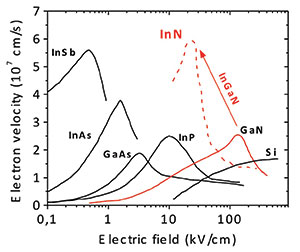
Figure 1: Electron velocity dependence on the electric field at room temperature in different semiconductors (taken from T. Palacios phys. stat. sol. (a) 206 1145 (2009)).
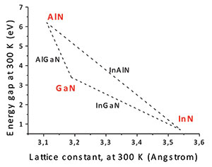
Figure 2: Energy gap dependence of III-Ns on the lattice constant.
We have selected InN because it sports the highest theoretical electron velocity of all commonly known semiconductors (see Figure 1). Consequently, HEMTs that are constructed with an InN channel have the best chance that nature can offer to excel in the field of ultra-high-frequency semiconductor electronics.
The operating speed of the HEMT also depends on the carrier transit time along the gate. Based on this, and the theoretical electron velocity, a switch from a GaN to an InN channel promises to increase the intrinsic current-gain cut-off frequency, fT, by a factor of 2.5, which should take this transistor into the terahertz range.
Hitting such high frequencies will be helped by the low electron effective mass in InN. This offers the prospect for ballistic electron transport, which could propel the device to even higher speeds. However, despite all this promise, there are yet to be any demonstrations of microwave InN-channel HEMTs due to detrimental dislocations in InN layers.
These imperfections result from the significant difference in the lattice constants of InN and GaN. To try and avoid such issues, we are proposing an InN strained channel grown on an InAlN buffer layer, with either indium or nitrogen polarity at the surface, or as a non-polar material. Thanks to the small difference in lattice constants of InN and indium-rich InAlN, it should be possible to perform coherent quantum well growth and ultimately create an InN-channel HEMT producing its theoretically predicted performance.
The two most common designs of III-N HEMT feature a GaN channel and a barrier layer made from either AlGaN or InAlN. The heterostructures for these devices are grown on a buffer layer, which is typically a semi-insulating GaN or an AlGaN back barrier.
One peculiar property of the polar hetero-junctions made from the pairings of AlGaN and GaN, or InAlN and GaN, is that they create a two-dimensional electron gas (2DEG) quantum well that is formed without intentional doping, due to the high spontaneous and piezoelectric polarization.
The piezoelectric polarization arises due to internal displacement of ion sublattices in the strained epitaxial layer, while spontaneous polarization results from a lack of inversion symmetry in the nitride crystal structure.
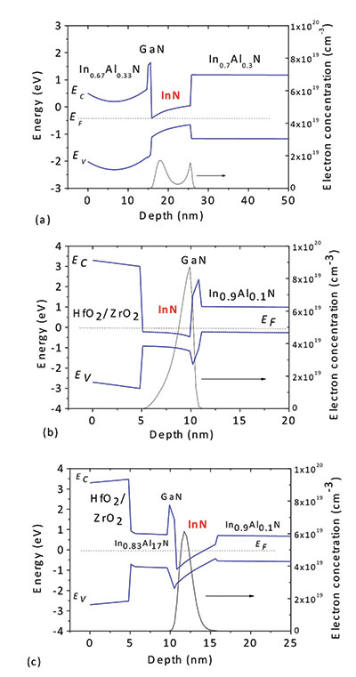
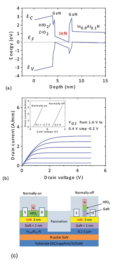
Figure 3: Calculated energy band profiles of normally-on InN-channel MOS HEMTs with (a) non-polar, (b) N-polarity, and (c) In-polarity orientation. For (a) the dielectric insulator is not shown and doping in the barrier is assumed to be 1019 cm-3. Elsewhere the non-intentional doping is 1015 cm-3. Calculated n2DEG = (a) 0.6x1013 cm-2, (b) 1.6x1013 cm-2, and (c) 1.2x1013 cm-2.
Selecting the best layers in the heterostructure is not simply a matter of considering the lattice constant, as it is also important to take into account the relative bandgaps of the materials (see Figure 2). Based on these considerations, we have chosen an indium-rich InAlN buffer layer, because it generates only a relatively weak compressive strain in the InN channel "“ to enable pseudomorphic growth of InN "“ and it has the highest energy gap difference compared to any other InAlGaN combination. Our relaxed InAlN buffer layer with an indium molar fraction of 0.7-0.9 is used in conjunction with a thin GaN spacer between the InAlN barrier and InN channel. Calculations suggest that this should ensure excellent confinement of a high-density 2DEG in epi-structures for all polarity cases (see Figure 3 (a)-(c)).
This combination will hopefully unlock the door to the exploitation of an InN HEMT. When state-of-the-art InN material is grown on GaN "“ rather than the buffer we are proposing "“ it has high electron concentrations and as a very thin (few nanometres thick) layer, it has a mobility that substantially lags that of theoretically predicted values. Our novel buffer and strained InN channel should lead to better HEMTs, by trimming the defect density in the quantum well and boosting mobility. To optimise this device, we will have to develop high-resistivity InAlN, which will involve exploring various acceptor and/or deep level compensation mechanisms.
Another avenue that we will have to explore is that of the different polarity orientations of InN-channel heterostructures, which could lead to different growth sequences, different interfaces, and new trapping mechanisms. Our team has already shown that polarity can be used to design normally-off HEMTs, for N-polar HEMTs, where a thin GaN cap creates a negative polarisation charge that depletes the channel (see Figure 4(a)). This effort is helping to pave the way to beyond-CMOS logic ICs, because it allows integration with normally-on HEMTs on identical substrates, thanks to highly selective etching of GaN over InN.
The realisation of ultra-fast logic and mixed-signal ICs based on InN HEMTs is clearly a long way off, but we have begun that journey. Achievements to date include the physical analysis of the concept; and practical breakthroughs, such as highly selective etching of GaN over InN, processing of MOS structures on (GaN)/InN, and the formation of the negative polarisation charge at the N-polar GaN/InN interface. If further progress is possible, then there might become a time when the InN HEMT lies at the heart of cutting edge technology deployed in circuits, imaging and communication in the terahertz domain.
E. Dimakis et. al. Appl. Phys. Lett. 97, 113520 (2005)
J. Kuzmik et. al.and A. Georgakilas IEEE Trans. on El. Dev. 58 720 (2011)
J. Kuzmik Appl. Phys. Express 5 044101 (2012)
J. Kuzmik et. al. Semicond. Sci. Technol. 29 035015 (2014)
K. ÄŒiÄo et. al. ASDAM 2014, Smolenice Castle, Slovakia, October 20-22, 2014