
Keeping cool with nanoceramics
Makers of solid-state lighting should turn to aluminium nanoceramics to cut the cost of thermal management in high-power LEDs
BY RALPH WEIR FROM CAMBRIDGE NANOTHERM
After dominating high-power lighting for decades, the incandescent bulb is losing ground to the LED. This alternative is making inroads in automotive lighting, warehouse and bay lighting, and being used as an industrial ultraviolet light source.
But there is a big problem with this solid-state source: As it moves further into the high power arena, the age-old issue of heat dissipation is rearing its head. Despite the enormous efficiency advantage of the LED over an incandescent source, more than two-thirds of the electrical energy is still wasted as heat, and if this is not removed it can cause catastrophic failure within the chip.
Although the proportion of energy lost as heat is higher in the incandescent source, dealing with it is actually easier. That's because the vast majority of the heat produced by this class of bulb is in the form of infrared radiation, which can dissipate into the air beside the glass enclosure. In contrast, the primary route for extracting heat from the packaged LED is conduction.
To conduct heat away as quickly as possible, LEDs are placed in contact with highly thermally conductive materials such as AlN. And further benefits in heat dissipation can be wrought with additional thermal management substrates, heat pipes and active or passive heat sinks.
Whatever approach is taken, however, the thermal path is only as good as its weakest point. And if the interface between the LED and the heat sink, or any other part, fails to conduct heat sufficiently well, the LED die will reach unacceptable temperatures. This will adversely affect the LED; shortening its lifespan, decreasing the light output, degrading the quality of light and ultimately causing device failure.

A packaged LED mounted on a Metal Clad PCB starboard
The LED industry's most common approach to thermal management is to mount the high-power chip on an AlN-based ceramic. This platform excels in two regards, combining superb thermal conductivity with good electrical insulation. The latter of these qualities is essential, because high-power LEDs often comprise a cluster of much smaller parts joined together by electrical connections.
Unfortunately, while AIN is more than up to the task of dispersing heat from a high-power LED, it has one huge drawback "“ it is extremely expensive.
Don't bank on this situation changing, because ceramic AlN is synthesized using exotic manufacturing techniques, such as the carbonthermal reduction of aluminium oxide and the direct nitridation of aluminium. Very few companies have the facilities required to produce AIN by these methods, hampering competition in the marketplace, while the innate brittleness of this ceramic leads to relatively low yields. To prevent breaking, the AIN ceramic packaging substrates tend to be supplied in square panels with sides that are 4-inch in length. Panels this small limit the number of LEDs built on a single tile and hamper attempts to realise economies of scale.
It can be argued that the high cost of AlN and its unsuitability for volume manufacturing is having a negative impact on the LED market, driving up the cost of packaged chips used in high-power arrays of devices. This has spurred designers to cast around for alternatives that sport the thermal conduction capabilities and good electrical isolation of AIN, but are cheaper and available in a form that permits integration into a high-volume LED production line.
An obvious candidate is aluminium, an excellent conductor of heat. This metal is cheap and available in an almost unlimited variety of shapes and sizes. However, attempts to anodize the surface of aluminium and create a dielectric layer between the LED die and the thermally conducting material (the aluminium itself), while trying to retain most of the thermal conductivity of the aluminium, have been an abject failure. Anodizing is incapable of producing a surface that is reliable and sufficiently uniform to act as a dielectric, and instead this treatment creates voids and fissures. These imperfections expose the aluminium beneath to electrical currents from above, creating a short circuit.
However, despite all these shortcomings, it would still be imprudent to dismiss aluminium. After all, this metal has many merits: it is cost-effective, readily available, lightweight and flexible. What's more, there are a wide range of suppliers of thermal management solutions using aluminium as a core part of their business, massively increasing the potential supply chain. All that is needed is to uncover a compatible dielectric coating. At Cambridge Nanotherm of Haverhill, UK, we have found a way to create such a coating "“ we employ a patented electrochemical process that transforms the surface of an aluminium sheet into a dielectric nanoceramic layer of crystalline aluminium oxide.
One of the great strengths of this approach is that the aluminium oxide "“ in the form of crystals that are bonded to the aluminium at the atomic level "“ ensures a clear "˜thermal path'. That is, the interface resistance between the alumina and the aluminium is small.
The size of these alumina crystals is on the nanoscale, with dimensions down to 30 nm. This permits the dielectric layer to be orders-of-magnitude thinner than anything else available. Consequently, heat has very little distance to go when travelling through the ceramic layer to the highly conductive aluminium beneath.
An additional advantage resulting from the tiny size of the crystals, and the process by which they are created, is that the dielectric layer is incredibly uniform, with no weak spots. Thus the dielectric remains intact, even when it is grown on thin sheets of aluminium that have to flex or bow during subsequent processing or in service.
The nanoceramic-aluminium composite produces a thermal conductivity of 152 W/mK, which is very close to that of just aluminium. Thermal conductivity of the nanoceramic layer alone is around 7.2 W/mK, an extremely high value by industry standards. Meanwhile the dielectric strength is a highly impressive 50 µV/m.
Note that the thickness of this nanoceramic layer can be tightly controlled, making it possible to tailor the dielectric of the thermal substrate to a particular product's breakdown voltage requirements. Another attribute of this nanoceramic is that it can endure extensive thermal cycling − from around -40 °C to around +250 °C − without degradation.
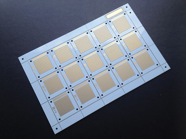
An example of a Nanotherm DM Metal Clad PCB
Our approach to making an aluminium oxide film stems from research dating back to the 1980s by our two co-founders, Pavel Shashkov and Sergey Usov, former researchers at the Moscow State University. This duo first focused on creating crystalline structures on the microscale. However, the unique properties of ceramic AlN only became apparent with the discovery that the manufacturing process could move into nanoscale.
The details of this process are closely guarded and ring-fenced by several patents. What can be revealed, however, is that the process involves ensuring extraordinarily precise control of the chemical aspects of the conversion process, and the application of energy required to power the conversion (which in itself pushes the limits of high-power electronics).
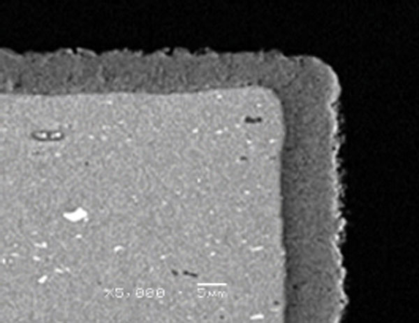
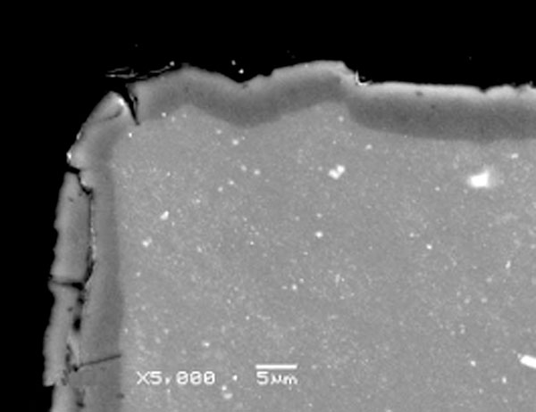
Nanotherm's process (top) forms an extremely dense layer of ceramic on the aluminium base, providing a reliable insulation. In contrast, anodising (bottom) forms a layer which is fractured "“ clearly not to be relied upon to prevent penetration of electrons through the dielectric layer.
When LEDs are attached to a substrate to improve thermal management, a circuit must be added. To realise this, we have developed a technology known as Nanotherm DM (Direct Metallisation), which involves using thin-film techniques to atomically bond a copper track directly to the nanoceramic surface of the aluminium. Tracks of standard thickness, such as "˜one-ounce' copper, are defined by electroplating.
This approach sets a new benchmark for circuit bonding. Thermal resistance can be as low as 0.02 K/W on a 1.5 mm board, while thermal conductivity between the top surface of the one-ounce copper track and a 0.6 mm aluminium alloy heat sink can hit 152 W/mK, according to the laser flash technique. This level of conductivity is in the same ballpark as metallised AIN.
Our technology also has the upper hand over the incumbent when it comes to the addition of vias in the thermal substrate beneath the die array. The vias provide electrical pathways between tracks on each side of the part, but in an AlN substrate they are expensive to fabricate and act as sites of mechanical weakness. Turn to our technology, however, and holes can be simply drilled through the aluminium before processing.
The nanoceramic coating then grows uniformly on the inside surfaces of the vias, providing electrical isolation, while the deposited copper provides electrical connections.
With the technical requirements taken care of, adoption comes down to cost "“ and it is here that aluminium nanoceramics win hands down. As a rule of thumb, aluminium nanoceramics are two-to-four times cheaper than AIN when they are implemented, in large panels, as a fully circuitized high-power LED packaging substrate. Note that this major cost saving is realised while exhibiting similar performance.
The cost saving is not surprising. It is partly because the approaches to producing an aluminium nanoceramic are far less exotic than that used for making ceramic AlN; and it is partly because the substrates can be far larger. Thanks to the robust physical properties of the aluminium and the ceramic layer, boards can be an order of magnitude larger than those for AlN, leading to significant economies of scale.
The LED market for nanoceramics is extensive, and it can be split into two distinct categories. The LED submount market for device packaging is an early adopter of the material as a replacement for AlN. The other key LED market is that associated with clusters, arrays, modules and chip-on-board LEDs. All of these have traditionally used AIN or epoxy-coated-aluminium printed circuit boards.
Manufacturers that are turning to nanoceramic aluminium are enjoying significant cost savings without compromising the quality of their products. In fact, they are finding that performance goes up, with a switch to epoxy-coated aluminium substrates with nanoceramics driving a 23 percent hike in lumen output while maintaining the temperature "“ and thus the lifetime "“ of the module. This means a reduction in die count is possible for the same lumen rating "“ enabling significant cost savings to the total bill of materials.
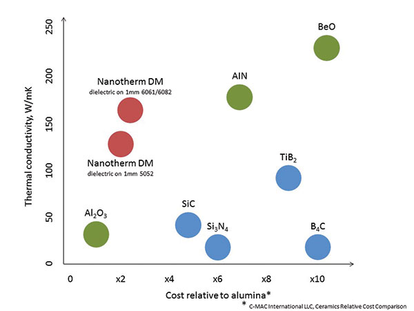
Material for the thermal management of LEDs should have a conductivity comparable to that of AlN, but be much cheaper. Cambridge Nanotherm's technology combines high thermal conductivity with comparatively low cost.
Trimming costs is a big deal, because it can help the LED market address one of the key sticking points that is holding up the mass market acceptance "“ initial purchase price.
Since full scale production started in 2014 demand has soared. To address this, over the next 12 months we are expanding our current factory, based just outside Cambridge, by adding additional manufacturing capacity. We are also planning to add new factories overseas, bringing our nanoceramics closer to target markets such as the US and Asia. These factories will be able to take advantage of lower production costs, making the nanoceramic proposition even more compelling.


