
Throwing away LED efficiency
Are parasitic currents in p-type layers holding back the efficiency of many commercial LEDs?
BY GREG TOGTEMA FROM LAKEHEAD UNIVERSITY AND K. SCOTT BUTCHER FROM MEAGLOW
Nitride-based LEDs are getting evermore efficient, enabling them to win deployment in situations demanding brighter light sources. At the beginning of the twenty-first century they produced enough lumens-per-Watt to backlight the screens of handsets, and now, thanks to a hike in efficiency, they are at the heart of solid-state bulbs for automotive and room lighting.
The tremendous gains in efficiency are setting this source apart from its incandescent counterpart, which ruled the roost through the twentieth century. Now outlawed in several countries due to its low efficiency, the incandescent generates light from a coil of very thin wire that is heated to such temperatures that it glows and emits some light and a high proportion of infrared radiation.
While LEDs are far more efficient than incandescent sources, they still waste a substantial proportion of electrical energy in the form of heat that drives up the temperature of the chip. This temperature must be maintained below what is known as the thermal limit to prevent a shortening of device lifetime.
To improve the performance of the LED, engineers aim to increase the efficiency of the chip while it operates at temperatures below the thermal limit. There have already been several refinements to LED design to succeed in this endeavour: thermal management has been improved through superior device packaging architectures, such as the introduction of a flip-chip design; heating within the chip has been reduced with better GaN buffer layers, which trim the density of lattice dislocations; and device efficiency has risen, thanks to improvements to the design of the active region, which increase the likelihood of radiative recombination between electrons and holes.
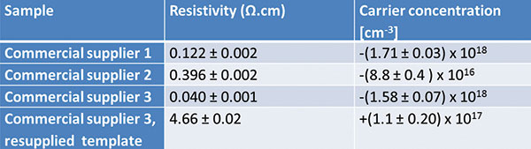
P-type templates provided by three different commercial suppliers had a carrier concentration that shows the dominance of n-type behaviour
Such efforts at improving the performance of GaN LEDs have already borne much fruit, leading to a period of diminishing returns. For example, adding more wells to the active region traps more carriers, but every additional well provides a smaller and smaller increase in light emission.
It is a similar story when driving an LED close to maximum current density, with each additional milliamp providing a smaller increase in light output. This stems from a decline in the efficiency of the nitride LED at higher current densities, which is a well-known problem referred to as droop.
Many researchers within industry and academia are trying to understand and address it, because droop-tolerant designs could increase the light emission and the efficiency of a chip.
Eliminating droop is challenging, with efforts held back by a lack of consensus over its cause. Many theories have been put forward, with some groups arguing that droop stems from non-radiative Auger recombination, while others are blaming undesired effects of indium incorporation or pointing the finger at carrier "˜spill over' across the heterojunction barriers.
Some of these theories have more persuasive arguments than others, but whatever the correct mechanism maybe, it is far from easy to build a droop-busting device. If Auger is the cause, the solution is to construct a high quality heterostructure that prevents electrons from scattering to energy states away from the quantum well conduction band minima. Meanwhile, if indium incorporation is not good enough, the growth temperature must be lowered "“ and if the quantum well heterostructure need optimizing, this will require redesign and testing.
Solving droop and addressing it is clearly very important. But it is not the only weakness that is dragging down the efficiency of the LED. It is also suffering from the poor quality of p-type doping in GaN, a little-known but important issue that has been discovered by our team from Lakehead University and Meaglow.
The role of p-type GaNStudies of droop will miss this, because they tend to focus on the electro-optical conversion efficiency, which dictates the amount of light that can be generated per milliamp of applied current. What we have found relates to the current
drift characteristics, which at least partially dictate the temperature rise per milliamp.
This rise in temperature varies across the heterostructure. The top p-type GaN layer used in an LED stack is typically one-to-two orders of magnitude more resistive than its silicon-doped, n-type counterpart, and this is where the greatest device heating occurs. But if the resistivity in this layer can be improved through the likes of better doping or a superior crystal structure, this could lead to a better LED.
There are many well-known limitations associated with p-type GaN that restrict LED performance. Firstly, carrier concentration "“ which determines both conductivity and luminosity "“ has an upper limit of around 1018 cm-3, due to self-compensation of the acceptor impurity. Secondly, the acceptor dopant, magnesium, must be thermally activated to remove the ill effects of hydrogen. But doing this can have its downsides, impacting the indium in the quantum wells and leading to a blue shift in emission.
On top of these issues, we have uncovered another problem. We have discovered that in a manufacturing environment, intentionally p-type material often has a carrier concentration that is not vastly higher than the residual background n-type concentration associated with oxygen impurities.
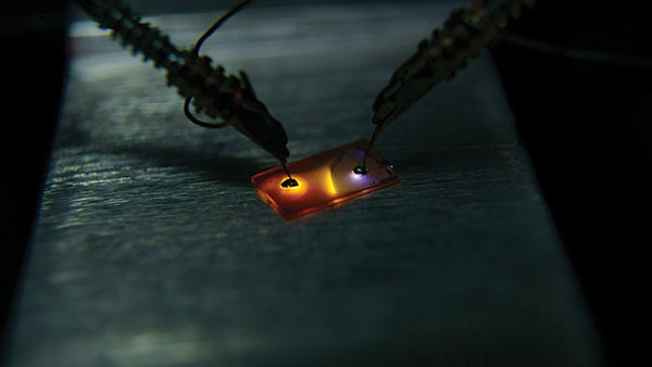
Yellow-orange InGaN test device. The probe to the left is on a high indium content n-type InGaN layer. The probe to the right is on the underlying p-type GaN template. The blue purple emission from the p-GaN probe is because of the slightly n-type surface oxide, one of several possible sources of n-type minority carriers.
Although hero measurements suggest that it is possible to grow undoped GaN with a background electron concentration of 1014 cm-3, this is far from typical. Far more common is that the hole concentration has to battle with a background concentration of electron donors of up to 1017 cm-3, even when no intentional n-type dopant is used.
We have recently investigated the impact of this background electron concentration, scrutinising characteristics of three commercially obtained p-type GaN templates from three different manufacturers. Using Hall effect measurements, we analysed the current flow in p-type GaN, finding that it is actually the background electron drift current that dominates the p-type drift.
That's not to say that the material did not have p-type characteristics "“ they are seen in luminescence spectra "“ but current flow was mainly due to n-type behaviour, with Hall measurements indicating that the material was n-type.
This shocking result led us to first check our equipment, using standard samples such as p-type germanium. We also spent considerable time confirming the quality of our ohmic contacts, but we could find nothing untoward, leading us to conclude that the measurements on these templates are not flawed.
How can this be, though, as the p-type doping level is higher than the n-type background? It's because the Hall measurements consider carrier currents, a product of the carrier density and the mobility − and the mobility of electrons
in p-type GaN is much higher than that for holes. In other words, when it comes to carrier concentration, compared to holes, electrons punch above their weight.
Many makers of nitride-based LEDs will be oblivious to this issue because they don't examine the electrical characteristics of their p-type GaN with Hall experiments, due to difficulties in interpreting the results on measurements involving an epistructure with many different layers. Instead, these device makers tend to use mercury probe capacitive-voltage (CV) profiling to check their materials' net carrier concentration − but this only determines the net charge across a depletion region. Such measurements are not influenced by carrier mobility, nor are they sensitive to the effects of carrier drift. All they reveal is that there is a net concentration of holes, which satisfies the manufacturers of LEDs that are unaware of the true nature of their GaN films.
In fact, these chipmakers are probably oblivious to the true hole current in their p-type layers "“ we have received films quoted as being a high
1017cm-3 of holes, but because of the high mobility of the electrons, the value given by Hall measurements is an electron concentration of about 1018 cm-3.
These findings indicate that the background oxygen levels influence material properties well before they impact net carrier concentration. This happens through the existence of a parasitic minority carrier current in the p-type GaN.
The good news is that it is possible to reduce background electron concentrations in undoped and p-type GaN by taking appropriate steps for MOCVD growth. These include reducing any discernable air leaks in the gas flow system; using purifiers for gas supplies and highly purified metal-organics; ensuring that water vapour formed from ammonia byproducts or metal-organics is properly purged from the system; and employing proper purging and a sufficiently long pre-growth baking regime, so that background oxygen carrying species, such as water, are eliminated prior to film growth. These are recommendations that many chipmakers are already well aware of, but their importance makes a difference at a much earlier stage than they probably realise.
Impacting LED performanceLED chipmakers should also be concerned about the parasitic minority carrier current uncovered by Hall effect measurements. Even if their p-type GaN is p-type, they will have a parasitic current present in the GaN p-type top layer of their LED stack. This means that in addition to the primary current in the p-type GaN that is associated with the transport of holes to the active region, there can be a significant minority carrier current of electrons heading towards the back ohmic contact of the p-GaN. The latter current makes no contribution to light emission, so impairs device efficiency.
In experimental labs the emphasis is on material quality rather than wafer throughput, so we expect low background levels of oxygen and minimal minority carrier currents − this might even be the case when background oxygen levels are not monitored on a regular basis. But for high-volume chipmakers that are churning out as many devices as possible, the lack of a proper method for measuring background oxygen levels may mean that this problem can slip by undetected, with device efficiency suffering in silence.
What is needed is an approach for monitoring minority carrier currents in p-type GaN structures. This information cannot be extracted from CV measurements, while Hall measurements are rather cumbersome. However, it should be possible to monitor carrier diffusion lengths in an industrial setting using optical pulses. This approach could be complemented by secondary ion mass spectrometry, a destructive, time-consuming approach that offers a direct measurement of oxygen levels.
One consequence of our work is that it begs the question: How big a problem is poor p-type doping in nitride LEDs? Well, it could be huge, based on the p-type templates that we have examined from three commercial suppliers. If LEDs were made that incorporated p-type material found in these templates, their LED efficiency would be compromised significantly. This is a wake-up call for the need to monitor the quality of p-type GaN.
One may also wonder if the parasitic minority carrier currents contribute to droop. It is not trivial to answer this, as it would require knowledge of the relative voltage dependence of the majority and minority currents, plus a modelling effort that accounts for barrier heights and other material and device characteristics.
Exploring this is surely a worthwhile endeavour − but one for someone else. Our aim, particularly at Meaglow, is to continue to look at producing indium-rich InGaN on p-type GaN. By studying templates of this material, we discovered some alarming issues relating to the nature of commercial films of this nitride. We now hope that by making others aware of this potential pitfall, LEDs will soon be free of this particular malady.


