
Europium propels the GaN LED into the red
Doping of GaN with europium enables a red LED to join forces with blue and green cousins and form a monolithic, full-colour chip
BY YASUFUMI FUJIWARA FROM OSAKA UNIVERSITY AND WOJCIECH JADWISIENCZAK AND FAIZ RAHMAN FROM OHIO UNIVERSITYLEDs have a sensational set of attributes. These small, highly efficient and versatile chips are now serving myriad roles, from space illumination to communication, gas sensing and displays. And performance continues to improve, as manufacturers strive to increase efficiency and lower cost, while researchers in academia and industry develop new materials and architectures for next-generation devices.
Since the invention of the LED, one of the targets of researchers has been to extend emission to shorter and longer wavelengths. Historically, this has been realised by varying the composition of the alloys used for making these solid-state emitters, but more recently it has involved changes to the thickness or the stoichiometry of the quantum wells.
For a decade or more the latter technique "“ compositional tuning, also known as band gap engineering "“ has been adopted for extending the emission of III-nitride LEDs into the ultraviolet and towards the green. This approach has yielded much success, with several groups reporting deep UV and green III-N LEDs. What's more, green laser diodes have been developed and launched to market. These triumphs beg the question: Is it possible to push the emission even longer "“ perhaps all the way to the red and beyond?
The pay-off of developing a red III-nitride LED would be huge. Although red LEDs are already available with the AlInGaP system, forming this with the III-nitride system would allow all three primary colours to be integrated on the same chip. Such a device would revolutionise the display industry, and would also find deployment in applications requiring a compact, full-colour light source.
Producing a red-emitting III-nitride LED is far from trivial, however. Stretching emission to longer wavelengths requires an increase in the indium content of the quantum well, but this goes hand-in-hand with plummeting efficiencies that originate from deterioration in crystal quality and increased alloy segregation.
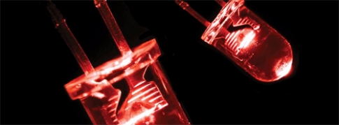
Figure 1. The first GaN-based red LED operating under current injection at room temperature. Europium-doped GaN is used as the active layer of the LED.

At the heart of the issue are opposing temperature requirements for the growth of indium-rich InGaN. Temperatures in the region of 1000 °C are needed to ensure the supply of sufficient nitrogen via the cracking of ammonia, while temperatures below 600 °C should be employed to prevent decomposition of the alloy.
However, armed with clever epitaxial growth techniques, it is possible to circumvent these problems. Trailblazing this approach has been Kazuhiro Ohkawa and colleagues at the Tokyo University of Science. In 2011, this team demonstrated that indium-rich InGaN can be deposited by altering the design of the MOCVD reactor: The substrate is held in a confined space, and ammonia flows by while heated to a higher temperature. These researchers also modified the design of the active region, doubling the number of quantum wells from five to ten. This enabled the epitaxial structure to relax, aiding indium incorporation.
These modifications to the growth and the architecture of the LED led to the fabrication of deep red LEDs. However, the output power of these 740 nm devices was only 2 µW. So one can conclude that a lowering of the growth temperature is not that promising an approach to making powerful red III-nitride LEDs.
A team from Toshiba's Corporate Research and Development Centre has pioneered an alternative way forward that appears to have more potential. Their device featured thin AlGaN interlayers inside each GaN/InGaN quantum well, and it emitted 1.1 mW at 629 nm. Although this output is much, much higher than that from devices reported previously by other groups, it still falls short of a practical device, due to its low external quantum efficiency of around 2.9 percent.
Another approach, pursued by many groups, is to build LEDs based on nano-columns. This makes it far easier to incorporate indium, but the downsides are low device efficiency and complicated growth and fabrication procedures.
Figure 2. Photoluminescence from europium-doped GaN. Emission peaks are assigned as the intra-4f shell transitions in Eu3+ ions.

There is also a radically different approach to making red LEDs: Doping them with trivalent europium (Eu3+). This ion is already widely used, providing a luminescent centre in red-emitting phosphors, such as europium-doped Y2O3 that is used in cathode ray tubes and plasma display panels. In these applications ions are doped in an insulator (host matrix), with red emission primarily resulting from charged particle and optical excitations.
One of us, Yasufumi Fuijiwara from Osaka University, is broadly adopting this approach, but taking a slightly different tack by doping europium directly into the GaN. This method has much promise, because europium-doped GaN has excellent luminescence properties in the red spectral region, resulting from the specific optical properties of rare-earth elements. This includes a sharp, intense, temperature-independent emission peak associated with intra-4f shell transitions.
One of the downsides of rare-earth excitation is that it is very sensitive to energy mismatch between the host and the doped rare-earth ions. Consequently, care must be taken when selecting the bandgap of the host. As a general rule, wider bandgap materials are preferred, because they provide a greater number of energy migration channels for exciting rare-earth ions. In fact, due to significant physical and chemical differences between the rare-earth element and the host atom it replaces in a semiconductor − including variations in ionic radii and electronegativity − the rare-earth ions often have to be considered together with the gap level they generate in the host. This facilitates the 4f-shell core excitation and de-excitation processes. Typically, rare-earth elements incorporated in the semiconductor are in the (3+) charge state. The rare-earth ion loses all 5d and 6s electrons to form ionic bonds, and the partially-occupied 4fn-shell provides multiple electronic energy levels for energy migration. It is between these levels that radiative transitions can occur. When doping GaN with the rare-earth elements, optically active centres are formed that exhibit temperature-stable, narrow "˜atomic-like' emission lines. The spectral position of these lines is defined by the spin-orbit splitting of electron states in the partially occupied 4f shell of the rare-earth-ion.
Figure 3. Electroluminescence of europium-doped GaN LED with different applied voltages.

GaN is a great host because it combines a direct bandgap with a high level of optical activity, even when it features a high defect density that would quench emission in other technologically important, but smaller bandgap, III-V and II-VI compounds. Another strength of using III-nitrides is that there is weak thermal quenching of radiative emission produced by the optically active rare-earth ion.
When Eu3+ ions are incorporated into GaN, they are substituted for metallic cations (Ga3+) and occupy sites with reduced symmetry. There is no contribution to the state energies from the odd-parity components of the crystal field, but electric dipole transitions between 4fn states are present, due to the admixing of opposite-parity wavelengths into multiplets.
We are not the first group to fabricate europium-doped GaN layers. In the late 1990s and early 2000s, a group from the University of Tsukuba, another from the University of Cincinnati, and a partnership between researchers at Ohio University, Sandia National Laboratories and the Lawrence Berkley National laboratory all formed such structures by either MBE, or by implanting ions followed by a post-implantation thermal anneal. Optical excitation resulted in stimulated emission from the europium ions, and electroluminescence resulted from two different device architectures: europium-doped GaN grown on p-type silicon and caped with indium-tin oxide; and a metal-insulator-semiconductor structure with indium, europium-doped GaN, and an n-type silicon substrate.
These devices produced red emission, but only under very high voltages. For the device capped with indium-tin oxide, voltages as high as 46 V were employed − and this produced weak emission, due to the low efficiency of the impact excitation of Eu3+ ions by hot carriers. One option for reducing the operating voltage is to turn to a device architecture with a p-n junction, which can inject the current into an active layer and realise energy transfer from host excitations to Eu3+ ions. The team from Osaka University has used MOCVD to investigate atomically controlled doping of rare-earth atoms in III-V semiconductors. They reported our initial success in 2009, when we grew europium-doped GaN layers with high crystalline quality, and demonstrated low-voltage, current-injected red emission from p-type GaN/GaN:Eu/n-type GaN LEDs (see Figure 1).
We have investigated room-temperature photoluminescence produced by the europium-doped GaN. Over the entire 2-inch wafer, bright red emission was produced, with peaks at 543 nm, 600 nm, 621 nm, 633 nm and 663 nm associated with the intra-4f shell 5D1"“7F1, 5D0"“7F1, 5D0"“7F2, 5D1"“7F4, and 5D0"“7F3 transitions, respectively (see Figure 2). The strongest of these peaks is at 621 nm, with a full-width-at-half-maximum of 1 nm. Note that there is no evidence for either band-edge emission, which would be expected at 361 nm for undoped GaN, or for defect-related blue/yellow band luminescence. This indicates that there is a very effective transfer of excitation energy from the GaN host to the Eu3+ ions that underpin the strong red luminescence.
Devices formed from europium-doped GaN, which otherwise have a structure that is similar to that of a blue LED, start emitting light at a forward voltage of just 3 V (see Figure 3). Similar to photoluminescence, the dominant emission peak occurs at 621 nm. A key observation is that under reverse bias, there is no electroluminescence − this implies that all the light generated when the device is under forward bias results from energy transfer from the host to the europium ions, with none stemming from impact excitation or ionisation of these species via hot carriers.

However, the emission produced by that generation of LED was very modest. At a 20 mA drive current, output power, integrated over the 5D0"“7F2 transition region around 621 nm, was just 1.3 µW, while the external quantum efficiency was 0.001 percent.
We have steadily increased the output of our LEDs by optimising growth conditions and device structures. Switching to growth at atmospheric pressure enhanced europium-specific emission, due to a combination of an increase in the number of optically active europium-ion centres, efficient energy transfer, and a further reduction of non-radiative processes in the GaN host. This propelled the output power integrated over the 5D0"“7F2 transition region to 17 µW at 20 mA; the corresponding efficiency was 0.04 percent.
Another lever to increasing LED output is to increase the thickness of the active layer. Power increases monotonically with active region thickness, due to increases in the number of europium ions, with a peak power at 20 mA of 50 µW for an LED with a 900 nm-thick active region. The corresponding external quantum efficiency for this emitter was 0.12 percent.
Further improvements have followed, with output power increasing to 93 µW at 20 mA − this is the highest value ever reported. This output corresponds to an external quantum efficiency of 0.23 percent, putting this device in the same ballpark as green-emitting, commercially available nitrogen-doped GaP LEDs.
At lower injection currents, the LED operates at an even higher efficiency, suggesting that the number of optically active europium-doped ions may be a bottleneck. We know from a recent study of ours on europium luminescence that there are at least eight different kinds of europium luminescent centres with different local structures that can coexist, and that the energy transfer from the GaN host depends strongly on the local structures. Due to this insight, we have devoted much effort on the selective formation of luminescent centres with efficient energy transfer. This has involved co-doping europium with other impurities.
One of the promises of a red-emitting nitride LED is that it can be integrated with a blue and a green cousin on the same substrate to form a chip that emits all three primary colours. We have taken a significant step towards this by employing selective growth to form red and blue emitters side by side. Our hope is to follow this up with a full-colour monolithic red-green-blue chip that can be used for screens and projection displays. This will be superior to the hybrid LEDs of today, due to lower cost, easier system integration and much better colour mixing.


