
Propelling The Power Industry With Single-Wafer Systems
Single-wafer systems combine great levels of uniformity with minimal maintenance and an easy route from development to high-volume production, making them ideal for the production of GaN-on-silicon HEMTs
BY SUDHAKAR RAMAN, SOMIT JOSHI AND GEORGE PAPASOULIOTIS FROM VEECO INSTRUMENTS
Companies manufacturing devices that meet these criteria are in an enviable position because the list of potential applications that they can target is growing ever longer. There are emerging opportunities for increasing efficiency in IT servers, electrical motors, electrical vehicle recharging systems, windmills and solar inverters.
The soaring demand for greater energy efficiency is coming at a time when many believe that the incumbent technology "“ silicon-based power devices "“ is reaching its limits. This is spurring the development of a new breed of power electronics, based on new materials that will set a new benchmark for energy efficiency.
Those that are pursuing this goal include teams of engineers at several integrated device manufacturers (IDMs), and also those that are working for industry cooperative groups "“ including the well-known imec that is based in Europe, and PowerAmerica, a new comer based in the United States.
PowerAmerica has been formed through a public-private partnership between the US Department of Energy, industry and academia, with the latter led by North Carolina State University. Highlighting the importance of advanced power device development, the Energy Department has pumped $70 million into PowerAmerica.
To develop a new generation of power devices that are smaller, far more efficient and capable of operating at far higher temperatures than those made from silicon, PowerAmerica and imec are turning to wide bandgap materials. Efforts of both institutions are not limited to new device architectures, and include the introduction of new manufacturing processes. The devices that PowerAmerica, imec, and many IDMs are developing are based on either SiC, grown on a native substrate, or GaN-on-silicon (GaN substrates are very pricy and limited in availability, so many developers of power electronics consider them unsuitable for device manufacture).

Figure 1. Photoluminescence mapping on an 8-inch GaN-on-silicon wafer reveals that the standard deviation in the aluminium composition in the AlGaN layer is 0.29 percent.
With a bandgap that is about three times that for silicon, these wide bandgap devices can deliver faster switching with less energy loss, a smaller component size and potentially greater reliability "“ attributes that lead to system-level benefits (see the panel "The promise of GaN-on-silicon" for more details).
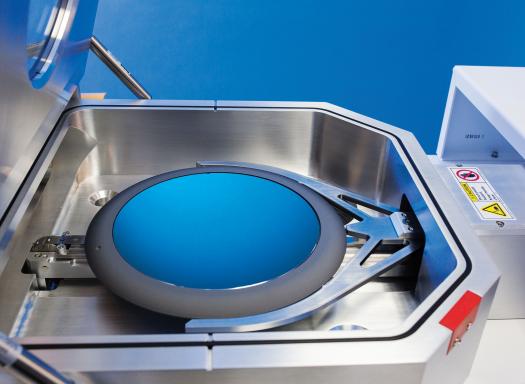
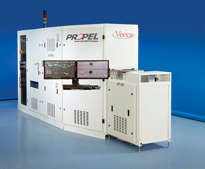
To speed the development of GaN-on-silicon power devices, our team at Veeco Instruments has developed the Propel PowerGaN single-wafer manufacturing system. It is based on the core MOCVD technologies used in our multi-wafer TurboDisc EPIK700 and MaxBright batch systems. The propel, a 200 mm-wafer-capable system, allows makers of power devices to leverage our many years of technical experience in MOCVD, as well as our market expertise.
Thanks to this, chipmakers purchasing the Propel are able to accelerate their development of next-generation GaN-on-silicon devices.

Figure 2. Triple-axis X-ray diffraction reveals the variation in thickness of the AlGaN barrier. This variation is two-to-three times less than it would be for an epiwafer produced in a multi-wafer system.
One of the biggest factors for determining the performance of GaN power devices is the quality of the epitaxial film. To optimize this, we advocate the use of single-wafer reactors, which have a proven and successful track record for rapid, cost-effective research and development. Compared to batch systems, single-wafer reactors provide a superior film quality of critical layers, much better run-to-run repeatability, higher production availability and a lower consumption of spare parts. Another strength is that in a cluster tool configuration, they can transition more cost-effectively into a high-volume production tool.
We have designed our Propel reactor to maximize production flexibility. One of its strengths is that it is designed to be integrated into a multi-chambered cluster tool on a single backbone. With this approach, the capital investment for development can be recouped when it is used to make products. This would follow a seamless transfer of the process recipe from pilot production to volume production.
Another attribute of the system is that although the reactor is currently configured for both 6- and 8-inch wafers, the architecture is extendable: When the industry roadmap requires a 12-inch capability, the platform will be able to address it in the future without losing productivity. There is also flexibility in terms of substrate material, as the Propel can be used to form GaN-on-SiC structures.
Advocating the use of single-wafer systems may raise a few eyebrows. Those of you that have been in the compound semiconductor industry for a long time will recollect that some of the first systems for production were single-wafer tools housing 2-inch wafers. Since then, to increase productivity and lower the cost-of ownership, MOCVD systems have increased in capacity by accommodating multiple wafers of larger sizes.

Figure 3. Run-to-run repeatability of a full HEMT structure; run-to-run repeatability of full stack thickness, AlGaN barrier thickness and aluminium composition, and thickness/composition uniformity.
Why, then, are we behind a switch back to single-wafer systems? Well, because history attests that it is the best way to increase productivity. In the silicon industry of the 1990s, the batch tool reigned supreme for performing the epitaxial processes for silicon-based ICs. In this era, the 130 nm/90 nm node took over from the 180 nm node, while the batch systems were left unchanged. This approach was viewed as a practical solution for transitioning from the development of the device to volume production.
It was a fine plan in theory, but a failure in practice. The repeatability and uniformity of the batch systems were unsatisfactory, problems that were exacerbated by the introduction of new technology, such as smaller design nodes and larger wafer sizes. After wasting much time and money, companies cut their losses by switching to single-wafer tools.
This transition worked out better than many expected, thanks to the configuring of single-wafer tools as a cluster tool system, easing the path to volume production. These systems, which provided an overall cost-of-ownership that is lower than that for batch tools, proved flexible enough to serve the industry over the next ten to twelve years.
Superior resultsThe superiority of the singe-wafer system is demonstrated in the far greater uniformity of the epilayers. Greater uniformity stems from the unique design of its wafer heating and gas injection subsystems.
Improving the uniformity of the layers is a major breakthrough, because it increases the device's performance and reliability. Properties of the two-dimensional electron gas that arises at the interface between AlGaN and GaN are determined by the thickness and the composition of the AlGaN barrier. This barrier influences the transistor's threshold voltage, on-state resistance and drain current − and to ensure a high yield, it is essential for it to have a highly uniform composition and thickness.

While this result is encouraging, process engineers working in high-volume fabs know that they don't just need highly uniform wafers now and again, but run after run after run.
Our system does not disappoint: Based on the Turbodisc family, it has unique architectural features and a stable, wide process operational space, enabling it to combine clean operation with excellent run-to-run repeatability. It is capable of carrying out more than 150 growth runs between preventative maintenance procedures, compared to typically 20 for a batch system.
In addition to the strengths already outlined, our single-wafer system offers faster run times and allows engineers to spend more of their time refining the IC design and the process recipe.
To drive the development of GaN-on-silicon technology for power electronics, we are providing Propel reactors, epiwafers and our expertise in MOCVD, in partnership with other industry associations and leaders.
Our industrial partners are working to improve the quality of the epitaxial layers, because this will improve device performance and increase yield. Their efforts are also being directed at developing advanced vertical devices, and developing new isolation modules that can increase the level of integration.
We hope that our efforts, and those of our industry partners, will help to position GaN power device manufacturers for successful product introductions in 2016, followed by a smooth ramp to high-volume production for GaN power devices in 2017. Ideally, these GaN-based devices will address the 600 V to 900 V operation range, where we anticipate the greatest demand for consumer and industrial applications.


