
SiC: Identifying imperfections with Raman spectroscopy
A revolution in Raman spectroscopy allows routine mapping of SiC wafers in little more than an hour.
Raman spectroscopy is a tremendously powerful technique for scrutinising SiC. It can determine different polytypes, quantify stress and strain, reveal carrier levels and identify the origin of defects.
But is this insightful form of spectroscopy available to all? Or is it only suitable for researchers with Raman expertise?
Acquiring Raman spectra is by no means a trivial task, because these signals are incredibly weak. The technique involves directing a monochromatic beam of light at a sample, collecting the back-scattered radiation, and passing this through a spectrometer. The vast majority of the light that is scattered from the sample will be at exactly the same wavelength as the incident source, but a very small proportion of it "“ perhaps a few parts in a million "“ will be at a slightly different frequency, due to the interactions of photons with atomic vibrations within the material under investigation.
In decades gone by, collecting Raman spectra would be the job of a dedicated experimentalist, skilled in the art of aligning optical components. They would toil away in an incredible dark lab housing a bulky triple-grating spectrometer. Every few hours, so long as they kept topping up their detector with liquid nitrogen, they could acquire a spectrum with an acceptable signal-to-noise ratio.
By the 1990s, the situation improved dramatically, thanks to the launch of a Raman microscope by Renishaw, a UK company headquartered at Wotton-under-Edge. Developed in partnership with the late David Batchelder of Leeds University, this relatively compact instrument featured holographic notch filters, which offered a neat solution to preventing the vast majority of the backscattered laser light from entering the spectrometer and overloading the thermo-electrically cooled detector.
Even with these advances, optics skills were still needed. Many labs would have more than one laser for their Raman microscope, allowing the experimentalist to select the best sources for a particular sample. To reconfigure the microscope so that it operated with a different laser required the replacing of one notch filter with another and the realignment of the instrument. With practice, this could be done within an hour, but for inexperienced users, it could take the best part of a day.
Another step-change in simplicity came after the turn of the millennium, with the launch of a new generation of Raman microscope.
"With the inVia [Raman Microscope], all the complexity is taken away by having an automated system," explains Ian Hayward, Raman Product Marketing Manager. "Switching between lasers is one click of a button, using a mouse."

By delivering high-speed mapping of SiC wafers, the Renishaw inVia Raman microscope enables a relatively quick identification of defects, polytypes, strain and carrier concentration.
This latest instrument, which continues to be refined, acquires spectra incredibly quickly. Now users not only take individual Raman spectra, as they would have done in the past, but also map areas in reasonable timeframes. For example, the mapping of a 3-inch SiC wafer takes just 75 minutes.
The substantial reductions in mapping times partly results from the availability of more powerful lasers, including a 532 nm source that is ideal for analysing SiC.
"532 nm is where you get your best bang-per-buck for laser power," explains Tim Batten, Applications Scientist at Renishaw. Acording to him, in the past these sources had an output power of typically 20 mW, but now 200 mW sources are readily available.
Helping to drive down acquisition times for Raman spectra are improvements in the efficiency of the detectors, and a higher level of automation that includes a maintaining of the optimal alignment of the optics.
The increased automation also allows the tool to be used more efficiently. "Now you can queue up a series of measurements and leave the instrument running overnight," says Hayward.
Making these measurements is incredibly straightforward, with the user only needing to know how to operate a microscope and use a PC.
"The main difficulty is analysis, and that depends on what you want to do," explains Batten. "We sell to a wide range of industries, and sometimes they'll have an expert there who sets up the initial analysis parameters, and writes a procedure." Technicians can then follow this, taking measurements day by day.
Supporting the SiC industryOften it is the interest of potential customers in Raman microscopy that triggers the team at Renishaw to investigate a particular use of this technique. That was certainly the case for SiC, with companies showing interest in using Raman microscopy to expose problems that could occur during the manufacture of substrates and the growth of epiwafers. Those interested parties included a vertically integrated firm. "For them, it is of great importance that they can determine where the problems are occurring, because they can remedy them," says Batten.
If one of the problems that they have involves the presence of more than one polytype within the material, this will come to light in the Raman spectra. That's because different polytypes have Raman peaks at different frequencies, due to differences in stacking geometry that produce atomic vibrations at different frequencies. As the Raman spectra for all the common polytypes are well known, it is possible to identify all the crystalline phases with a SiC film.
"You can also identify the orientation of the grain," says Hayward, "because you have a polarised laser, and you can analyse the polarised Raman light."
As well as the polytype, the vibrational modes within the crystal are influenced by the local environment of the atoms in a unit cell. So the spectra can uncover strain, defects, and damage to symmetry. "As a result of being able to measure strain, we are also able to infer stress in the material," explains Batten.

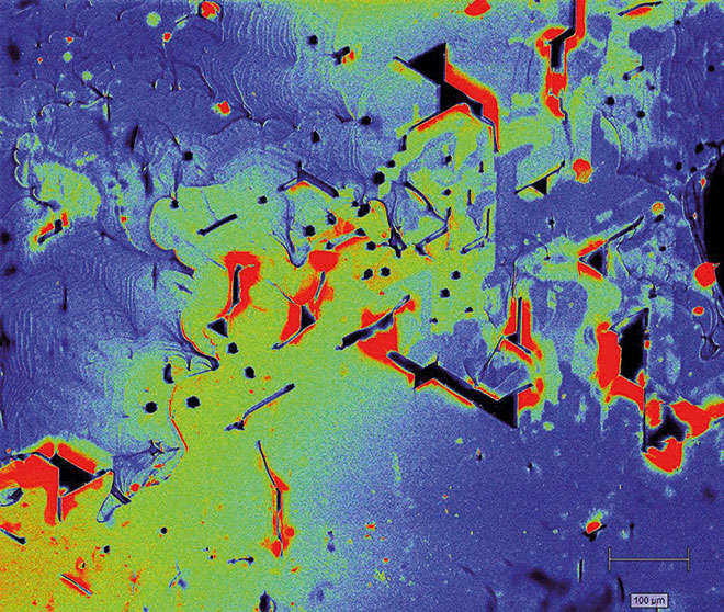
A comet defect. The image show the 4H- SiC substrate (green), the 4H-SiC epilayer (blue), and 3C-SiC inclusion (red/orange). Dimensions of the mapped region are 70 µm by 25 µm by 7 µm.
Some of these Raman peaks are electronically sensitive, with their position and peak width influenced by the free carrier concentration. This allows spectra to reveal the type of doping, and also its level. "I think it is difficult to be very accurate with those numbers," warns Batten. "Normally, to get the best values, people use a mixture of Raman and PL. This is fine as our instrument can also collect PL."
A great strength of the Raman technique is that it can determine the quality of material beneath the surface. "Effectively, all we are doing is mapping a surface, and then adjusting our focus into the material, and repeating the measurements while going deeper, to create a cube rather than a rectangle of data," says Batten.
"By having the three-dimensional capability, it means that rather than saying that there is a carrot defect there, we can say that it's a carrot defect and it originated from this location," explains Hayward. This allows engineers to distinguish between defects originating in the epitaxial layers, and those that can be traced back to imperfections in the substrate.
The resolution of the inVia Raman Microscope depends on the magnification of the objective lens. With the lens offering the highest magnification, later resolution is limited by diffraction, and it cannot exceed about 300 nm. Meanwhile, the depth-wise resolution, which varies with the refractive index of the material, and is of the order of a micron in SiC.
Classifying defects is possible with Raman, but it can also be carried out by various other techniques. "I think with Raman, one of the nice things is that the measurements are quite quick, so we can quickly classify them," says Batten.
Modest requirementsHeads of SiC labs and fabs that are considering installing this tool will be glad to hear that its needs are very modest. The instrument can be placed in a space where variations in temperature can be as high as a few degrees, and thanks to an enclosure, there is no need to turn off room lights when making measurements. Another attractive feature is that, for the vast majority of measurements, there is no need to place the instrument on a vibration isolation table. That's partly because the inVia is positioned on an isolation baseplate that keeps all the elements in position; and it is partly because optical stability is aided by a very careful design of the instrument, with all components mounted to a back plane, an architecture that minimises their relative movement.
Renishaw prides itself on looking after its customers. After installing the instrument, recipients receive a great deal of support in learning how to use the inVia microscope. This begins with a couple of days of on-site basic instruction directly following installation, and continues with more detailed training courses.
"We are running a course called Raman Revealed "“ we normally run it about twice a year," explains Hayward. "Customers or potential customers can come and learn how to use the instrument in detail. Our applications experts explain why you would do things in a certain way, the benefits of certain lasers, and how they would approach addressing a sample they hadn't come across before."
Simplifying the use of the instrument has made it accessible to a broader range of researchers and technicians, who benefit from software that is far easier to use than its predecessors. This software can gather vast amounts of data, due to the opportunity to map large areas and volumes of material. The data sets can easily be 100 GB, putting strain on data storage. "I've collected some two terabyte data sets. You could fill a hard drive every couple of days," remarks Batten.
An approximately 1 mm2 Raman image revealing inclusions of 6H-SiC, 3C-SiC or silicon (red), voids (black) and strain distribution (red).
The opportunity for statistical analysis is unleashed with the larger data sets. "A more powerful technique to analyse data is to look for variations and trends," says Batten. "Before, we were using very simple qualitative measurements, say peak width or peak position or peak intensity."
Potential users will find the ease of acquiring so much data appealing. However, they might be reluctant to invest in a Raman microscope, feeling that if the alignment of the instrument were to go astray, they might not notice, or would not know how to correct this issue. There is no need to worry about this, however, because the inVia Microscope has a health-check feature that can gauge the condition of the instrument. "If there are any health-related issues, it is possible for someone from the UK office, for example, to log on to the instrument remotely over the internet and perform any necessary adjustments."
This level of support will be welcome by those considering the inVia microscope for studying SiC "“ and also for those that are thinking of using it for scrutinising other compound semiconductor materials, such as GaN.
One of the great strengths of GaN, and also SiC, is that it allows the fabrication of devices with far higher operating temperatures than those made from silicon. To understand the capabilities and limitations of these wide bandgap devices, there is a need to accurately measure the local temperatures within these devices. "[Raman] gives you a very accurate temperature of a small volume, whereas if you use something like infra-red, you probe quite a large volume, so you massively underestimate the peak temperature," says Batten.
LEDs and lasers could also benefit from this approach to measuring device temperature, and Raman may also be a useful tool for measuring the strain within these devices, which may be formed by hetero-epitaxial growth. So there are clearly many opportunities for using Raman within our industry, and with acquisition times that are a fraction of what they were in the past, this technique has more appeal than ever before.


