
Boosting Normally-Off Power Switches
To lower losses in power conversion units, European project HiPoSwitch has established processes and infrastructure for low-cost manufacture of GaN-on-silicon HEMTs.
BY JOACHIM WÜRFL FROM THE FERDINAND-BRAUN-INSTITUT (FBH), BERLIN
At the global, national and local level, efforts are being directed at curbing carbon dioxide emissions and making the very best use of all energy resources. Although there are many ways to do this, they all involve using electrical energy as efficiently as possible.
This is by no means a trivial task. The rise in renewable sources has led to growth in energy generated in a DC form, although this is still overshadowed by AC sources. One must also note that transferring electricity from its point of generation to where it is consumed tends to involve stepping up and down the voltage, and while many appliances can be directly plugged into a power supply, electronic goods often have transformers that are built in to them to provide a low-level, DC source.
For efficient use of energy, the conversion of electrical energy at all these points in the chain from generation to consumption must be carried out with minimal losses. And if these energy converters can also be made smaller and lighter, they will be better at serving some emerging high-tech applications, such as mobile, air-, and space-borne systems.
A very promising class of device for meeting these demanding targets is the GaN-based power switching device. It has great material characteristics, including a high breakdown strength and electron velocity, and compared to the silicon incumbent, it can turn on more efficiently, be more compact, and switch at far faster speeds.
These attributes translate into a superior performance for the power converter. Those that incorporate GaN transistors have less than half the losses of existing technologies and make conversion efficiencies of over 98 percent practical. If these converters were widely deployed, it would lead to tremendous savings in primary energy consumption.
A simple calculation can illustrate the level of these savings. In Europe, more than 3000 terawatt hours of electrical power are generated every year. Assuming that only a quarter of this electricity is converted to different energy levels and efficiency is increased by just two percentage points, this would allow at least two coal-fired plants to be turned off. In other words, this emerging technology can have a huge impact.
To address the technological challenges of making devices with this wide bandgap technology, the European Community has funded a three-year project called HiPoSwitch. Kicking off in 2012, this effort, backed by €5.6 million, has focused on the development of GaN power switching transistors as the centre-piece of modern electronic energy conversion systems.
Co-ordinated by FBH (Ferdinand-Braun-Institut, Leibniz-Institut fuer Höchstfrequenztechnik), this programme involved eight institutional and industrial project partners and succeeded in developing GaN prototype, normally-off, power switching transistors. The manufacturability of these devices on a large-scale industrial production line has recently been demonstrated within this project.


Figure 1: Performance of 60 mΩ GaN power switching device fabricated on a SiC substrate (left); pulsed output characteristics (1 µs pulse duration) (right): Evolution of dynamic on-state resistance and drain leakage with drain voltage.
Together, the complimentary players in the HiPoSwitch consortium spanned the full value-added chain towards an efficient energy conversion system (see the panel "Roles within HiPoSwitch" for details). Expertise ranged from epitaxial wafer growth to device design, processing, circuit design, low-inductance packaging and the final implementation of developed devices into a converter system environment. Tasks that were performed included thorough device characterization − static and dynamic performance and reliability testing.
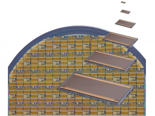
Efforts focused on the industrialization and rapid exploitation of the results. For example, during the project, the diameter for GaN-on-silicon epiwafers increased from 4-inch to 150 mm and finally to 200 mm. This eases the transfer of this new technology to a commercial process line.
Starting conditionsThose working within the project did not have to start from scratch − instead, they were able to draw on their previous experiences in GaN microwave and power-switching transistors. However, the power switching devices were not ready for system implementation at the outset, because they lacked the requested stability and current-switching ability, and were also suffering from dispersion effects upon power switching.
The HiPoSwitch programme tackled these issues, focusing on the development of normally-off GaN power-switching devices for 600 V operation in a 3 kW telecom rectifier demonstrator system. The switches for this were developed on silicon and SiC substrates, enabling a fair comparison between the two different substrate types, based on nominally the same device architecture.
EpiGaN, working closely with MOCVD tool manufacturer Aixtron, developed and fabricated GaN epitaxial structures on silicon substrates with ultra-low leakage currents at 650 V and breakdown higher than 1000 V, while FBH focused on GaN-on-SiC epitaxial growth. Manufacture on SiC substrates was never intended − transfer to silicon substrates would follow, allowing a trimming of production costs and improved manufacturability.

Table 1. GaN transistors are superior to their silicon counterparts on many fronts.
For the continuous optimisation of normally-off GaN HEMTs on silicon substrates and the benchmarking of them against GaN-on-SiC equivalents, EpiGaN constantly delivered 4-inch GaN-on-silicon wafers to FBH. In parallel and in close cooperation with Aixtron, wafer diameters were increased from 150 mm to 200 mm, a necessary step towards cost-effective industrial production. At its Austrian location in Villach, chip-manufacturer Infineon implemented the newly developed GaN technology on its silicon process line, enabling industrial production of these power semiconductors.
All devices for the final demonstrator were fabricated on FBH´s 4-inch GaN processing line and assembled in Infineon's low-inductance ThinPak housing. These transistors were designed for 600 V power switching with a very limited dynamic on-state resistance increase. Another target was a turn-on resistance below 75 mΩ, which turned out to be challenging.
During the course of the project, devices strongly benefited from a combination of significant advancements in GaN epitaxial growth on SiC and silicon substrates, and an improved understanding of dynamic device behaviour. Thanks to this, at 600 V the dynamic on-state resistance increase during power switching plummeted from a factor of 100 at the beginning of the project to just 1.25 after its completion. Demonstrator chips, which featured a gate length of 214 mm, were able to switch up to 120 A if operated at pulsed conditions (see Figure 1 for details, and table 1 for benchmarking of devices against Infineon's state-of-the-art Si-CoolMOS devices, which had nominally the same turn-on resistance).


Figure 2: Comparison of GaN-on-silicon and GaN-on SiC devices designed for 60 mΩ turn-on resistance. Static transfer characteristics (1st); pulsed output characteristics of 60 mΩ normally-off devices taken at a gate voltage of +5 V (2nd and 3rd).
Tremendous improvements in the performance of GaN devices during the HiPoSwitch project were enabled by excellent co-operation between the partners. Sharing of simulation results, measurements and reliability data underpinned advances in critical areas, such as epitaxy and device processing. A key part of this was the comprehensive investigations of drift and degradation effects by researchers at the University of Padova and the Vienna University of Technology.
One of the most fascinating parts of the entire programme involved the comparison of normally-off GaN HEMTs fabricated on GaN-on-silicon and GaN-on-SiC substrates. Both classes of transistor were formed using nominally the same epitaxy of the active layers and an identical processing sequence. Normally-off behaviour is quite comparable, with turn-on at about +1 V (see Figure 2). As expected, the maximum drain current capability is higher for the SiC-based devices, and inferior thermal properties of the silicon-based transistors are apparent when HEMTs are driven into saturation. However − and this is very good news − there is not a significant difference in the behaviour of both types of device when they are operated at an on-state bias point that is typical for an energy converter.
The systems-level partner in HiPoSwitch, Artesyn of Vienna, Austria, has used the GaN-on-silicon HEMTs to build a 3 kW rectifier (see Figure 3). The resulting unit, designed for telecommunication applications that include cellular base stations, converts line voltage to DC with an efficiency of 98 percent. Thanks to this increase in efficiency, this rectifier can cut down conversion losses by 50 percent compared to the more conventional converters. Part of its strength stems from the specialized switching topology, which is matched to the properties of the GaN switching transistors. The result is great performance at the system level, realised by units that are smaller and lighter than existing converters. They can address a broad range of applications, including those related to aerospace.
In addition to preparing GaN to go to market, the HiPoSwitch project excelled on other fronts, including the development of completely new techniques and processes. Work carried out by researchers at Vienna University of Technology and the Slovak Academy of Sciences in Bratislava led to successful testing of promising ideas for producing semiconductors based on MISFET approaches. The transistors that resulted, which feature a novel epitaxial layer structure, demonstrated true inversion-type, normally-off behaviour. Producing a turn-on voltage of +1.5 V at a current capability of 0.7 A/mm device width, the transistors open up new possibilities for the manufacture of low-leakage, normally-off GaN devices.

Figure 3: 3 kW telecom rectifier powered with prototype GaN transistors mounted in ThinPak housings.
One of the triumphs of HiPoSwitch is that it will ensure the availability of GaN power switching technology within Europe in the next couple of years. These chips are destined to incorporate enhanced functionalities and will underpin the introduction of very high switching speeds. After this, there will be a move to monolithic integration of a driver and free-wheeling diode, which will unlock the door to a new wave of improvements, based on even higher conversion speeds and smaller conversion systems.
As this happens, novel power switching architectures will be tested and unleashed. It is expected that this will include the introduction of vertical devices, which have already been explored in HiPoSwitch. FBH and Infineon, for example, have already developed quasi-vertical GaN device topologies that offer the possibility to realize either source-down or drain-down devices. This indicates that the advances made by HiPoSwitch look set to leave a lasting legacy.


