
Slashing the cost of the SIC MOSFET
BY SUJIT BANERJEE, KEVIN MATOCHA AND KIRAN CHATTY FROM MONOLITH SEMICONDUCTOR
Power engineers are striving to fulfil an ever-increasing demand for compact, high-efficiency power conversion systems. To succeed in this endeavour, they are considering the use of advanced power devices, such as SiC power MOSFETs that enable an increase in operating frequency, a shrinking of passive components and a trimming of the heat sink size. Although SiC MOSFETs retail for far more than the silicon IGBTs that they replace, savings at the system level and an increase in overall performance overshadowed this.
At Monolith Semiconductor of Round Rock, Texas, we believe that engineers should not have to pay a great deal more for SiC MOSFETs than silicon IGBTs, and we have introduced a new business model that will enable this, based on the manufacture of SiC devices on 150 mm silicon lines. We expect this move to slash SiC MOSFET costs by 80 percent within the next five-to-eight years, a move that will enable these devices to reach price parity with silicon IGBTs. This should unlock the door to a market worth more than $1 billion a year, according to analysts from Yole Development, Gartner and IHS.
Our cost savings are enabled by the recent availability of larger wafers. Not that long ago, the vast majority of SiC devices were produced on 100 mm wafers, using low-volume, dedicated fabrication facilities. This limited the availability of SiC MOSFETs, which retail for high prices. Savings are possible by turning to the high-quality 150 mm SiC substrates and epitaxial wafers that have been offered by suppliers over the last few years. Armed with these, there are benefits that extend beyond lower epitaxial costs per unit area, and include those associated with the manufacturing of SiC devices in 150 mm fabs.

Figure 1. The off-state and on-state performance of Monolith Semi's SiC MOSFETs, which have an on-resistance of 50 mΩ and blocking voltage greater than 1200 V.
Fabs that might be suitable for this include those that do not have an established, dedicated SiC line. After considering the specific requirements for SiC MOSFET processing, we have concluded that more than 90 percent of SiC device processes are compatible with processes that are available in a silicon CMOS fab. This means that by adopting properly designed process integration techniques and introducing a few SiC-specific tools, it is possible to fabricate SiC MOSFETs in silicon CMOS fabs with the same set of tools and processes that are used for processing silicon wafers at high volumes.
Such a move will dramatically change the paradigm for producing SiC devices, by opening up the opportunity for low-cost manufacture on fully depreciated, high-quality silicon fabs. It is a path that we are taking that has previously paid dividends for the makers of silicon power discretes and ICs − over the last two decades, they have exploited this fabless model and slashed the cost of silicon devices.
Our partner for manufacturing SiC MOSFETs on 150 mm wafers is X-Fab, which has a line near to us in Lubbock, TX. By working with them, we believe that we can immediately reduce the manufacturing cost of SiC MOSFETs by 40 percent. This will result from a combination of savings associated with the costs of manufacturing, and that of the SiC epitaxial wafers sourced from an external supplier; and gains on the gross die per wafer, and the expected die yield (see table 1). By the start of the next decade, our model suggests that manufacturing costs could plummet to below 20 percent of what they are today.
This model highlights that the price of the epiwafers dominates the cost of the SiC MOSFET. The quality of the epiwafer is similar for 100 mm and 150 mm products, but supply of the latter is limited to just three vendors: Cree, Dow Corning and II-VI. In contrast, between eight and ten vendors are offering 100 mm SiC wafers.

Figure 2. Monolith's MOSFETs, switched at 700 V and 30 A, produced a total switching loss per cycle of less than 0.5 mJ − an order of magnitude lower than that for a high-speed silicon IGBTs
However, thanks to investment in 150 mm SiC substrates and epitaxy, this state of affairs will change − additional suppliers will join the ranks, and existing ones will increase their capacity. As has been the case for 100 mm SiC wafers, this expansion in the supply base for 150 mm SiC materials will drive down prices. During the next five years it is possible that prices will fall to, or even below, those of today's 100 mm wafers.
This expectation should not raise eyebrows, because this is what has happened in the silicon and sapphire wafer markets, where growing volumes have gone hand-in-hand with falling prices and an increase in the number of suppliers. Further falls in SiC MOSFET production costs will result from an increasingly mature manufacturing process that will drive up yields and enable smaller die size.
We are not alone in claiming that the cost of producing SiC MOSFETs will plummet during the coming years. Anant Agarwal, a Senior Advisor for Wide Bandgap Technology in the Energy Efficiency & Renewable Energy division of the US Department of Energy, predicted last year in a presentation to delegates at the Materials Research Society that the cost of the SiC MOSFET has the potential to drop well below that of the silicon IGBT in the next five years. And the rate of price decline may be even faster than we expect if the 200 mm SiC substrates that have been demonstrated by II-VI are manufactured in significant numbers.
To make low-cost SiC MOSFET manufacturing on a 150 mm silicon line a reality, we have assembled a team of experts with complementary skills. Some of our engineers have expertise in SiC power devices, while others have an intricate knowledge of high-volume, fabless manufacturing of high-voltage silicon devices. While the concept of processing SiC wafers on a CMOS line is quite simple, it is by no means trivial to implement this in a manner that delivers success.

Figure 3. Results from accelerated testing of our gate oxide at 300°C indicates a lifetime of more than 100 years at the expected operating voltage of less than 25 V.
We have developed SiC diode and MOSFET designs and process that are compatible with a 150 mm CMOS production line and do not disrupt the high-volume silicon production that is running on the same tools. To realise this, we thought very carefully about how to integrate well-established CMOS processes with our SiC MOSFET process flow. The devices that we make, which offer excellent performance and reliability, exploit well-established, high-voltage device design techniques that are based on decades of silicon knowledge.
The primary near-term target markets for our SiC diodes and MOSFETs are photovoltaic inverters, datacentre power supplies and electric vehicle chargers. Looking further ahead, we anticipate opportunities in automotive traction inverters and motor drives.
Based on this outlook, our initial products are targeting blocking voltages ranging from 900 V to 1700 V and on-state currents between 20 A and 50 A. One example of such a product is a MOSFET that combines an on-resistance of 50 mΩ with a blocking voltage greater than 1200 V and a switching loss per cycle that is an order of magnitude lower than that of high-speed silicon IGBTs (see Figures 1 and 2 for further details of the device).
Holding back MOSFET sales are concerns over device reliability. Some power engineers have reservations related to either the gate oxide lifetime or the high-temperature threshold-voltage stability.
Our SiC MOSFETs address these concerns by delivering tremendous reliability at high temperatures. What's more, we have taken advantage of the excellent quality control of X-Fab's automotive qualified CMOS line. This has enabled us to demonstrate reliable, stable SiC MOSFETs.
According to high-voltage accelerated testing of our SiC MOSFET gate oxide at 300°C, wear out lifetimes are similar to those for silicon devices. Accelerated testing of our gate oxide at 300°C indicates a lifetime of more than 100 years at the expected operating voltage of less than 25 V (see Figure 3). We have also verified a stable threshold voltage at 175°C − 750-hour tests at a gate-source voltage of -10 V indicate a shift of less than 100 mV (see Figure 4). We are now working toward full 1000-hour qualification testing at 175°C.

Table 1. The cost of manufacturing SiC MOSFETs in a dedicated 100 mm SiC fab is far higher than that involving a 150 mm CMOS foundry. In the foundry, costs are considered for 2015 and for within next five-to-eight years, during which time the supply chain will matures. For the matured cost model, it is assumed that the number of good dies in a wafer will increase by 50 percent as the technology and processes mature. The cost model considers: the cost of SiC epitaxial wafers from an external supplier; the manufacturing cost; the gross die per wafer (using 5 mm edge exclusion); and the expected die yields (assuming the same for 100 mm and 150 mm in this analysis). For 100 mm wafers, a low-volume (approximately 1000 wafers/month), dedicated SiC fab is assumed and for 150 mm wafers a shared high-volume (roughly 20,000 wafer/month) CMOS foundry has been assumed.
These results highlight the promise of our low-cost approach to making high-quality MOSFETs. We are now scaling our SiC MOSFET process to the production of 100 A die capable of handling 900 V, 1200 V and 1700 V. These products will serve in high power modules that will help to drive increasing adoption of SiC devices in power electronics.
The authors acknowledge the support of ARPA-E, ARL, DOE, PowerAmerica, Xin Wu (UTRC) and NIST.

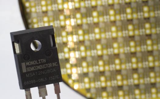
Figure 4. Stable threshold voltage at 175°C − 750-hour tests at a gate-source voltage of -10 V indicate a shift of less than 100 mV. Full 1000-hour qualification testing in progress. Monolith Semi’s 150 mm SiC MOSFET wafer out of the fab, and packaged MOSFET sample.


