
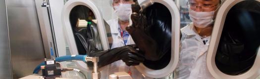
Technical Insight
Building the ICs of the future
The key to producing novel ICs with high efficiency and great functionality is to employ CMOS foundry process flows for the monolithic integration of silicon and III-V devices
BY DAVID KOHEN, ABDUL KADIR, KENNETH LEE, FAYYAZ SINGAPOREWALA AND EUGENE FITZGERALD FROM SINGAPORE-MIT ALLIANCE FOR RESEARCH AND TECHNOLOGY
Predicting the future is never easy. But it is a good bet that it will involve smart cities, smart homes and the Internet of Things − and underpinning all of this will be an increasing number of interconnected electronic devices.
To make this happen, the electronic devices will have to contain sensors that transmit data wirelessly to a control centre. This means they will have to combine RF capabilities with a small form factor and low operating power. A neat, promising approach to fulfilling all of these objectives is to make a single chip that unites the capabilities of silicon CMOS with those of III-V devices.
Despite its attractiveness, today the monolithic integration of silicon and III-V devices is not that common. Most commercial products are made by taking silicon CMOS chips, plus those based on III-Vs, and bringing them together in a single package. With this system-in-a-package approach, III-V and silicon CMOS devices are fabricated on separate wafers, before being bonded and connected by various methods, including through-silicon vias and bump bonding.
There are several drawbacks with this system-in-a-package approach, including a large form factor and a lower efficiency that stems from high interconnect losses. But these weaknesses could be addressed by turning to monolithic integration: a high performance and a small form-factor are possible when interconnects between III-V and silicon devices are shortened, so that they are comparable with those in conventional CMOS processes. For mature process nodes, CMOS interconnect distances are typically shorter than 5 mm − orders of magnitude lower than those associated with a system-in-a-package. Realising this level of integration slashes interconnect losses and reduces latency between different circuit modules. Self-sensing and self-tuning circuits can follow, enabling the serving of a range of new applications.
Just one of many examples of a technology that could benefit from the monolithic integration of different materials is the digital CMOS circuit. Access to ultra-efficient devices in a small form-factor could enable real-time adjustments at far higher rates "“ and this could address small and transient mismatches or non-linearities in analogue/RF or optical circuits constructed with III-V devices. Hybrid circuits would also be able to operate with greater stability and less noise. A significant increase in circuit functionality, complexity and performance could follow, realised without having to resort to a shrinking of device dimensions and a hike in transistor count.
Success with the monolithic integration of InP HBT and silicon CMOS technologies has been accomplished through the DARPA-funded COSMOS programme (and the subsequent DAHI programme). However, although the approach developed by this effort is technically feasible, integration took place in a research environment. Consequently, the advances that were made failed to offer a clear and ready pathway to scaling up production to high-volume markets.
To drive the industry adoption of a novel IC platform incorporating new materials, there has to be minimal disruption to existing CMOS foundry and processing infrastructure. These are the objectives that our team from Singapore-MIT Alliance for Research and Technology (SMART) set itself, and this has led to the development of a SMART Low Energy Electronic Systems (LEES) integration scheme. At its heart is a production process that begins and ends with standard processing at a silicon foundry, and also involves a series of growth steps associated with the growth of III-Vs on silicon.
Later on in this piece, we will describe our process in greater detail. But before we do this, let us first make the point that the advantages of our technique are not limited to smaller interconnects. Benefits also include the seamless integration of digital logic with III-V devices, which are best suited for photonic, opto-electronic and wireless electronic functions. Products that could result from this complementary marriage of materials include: intelligent LED lighting systems, which could feature integrating adaptive controls; high-speed wireless optical systems (Li-Fi); networks of self-powered drones for logistics and monitoring; and self-powered wearable electronics. There is also the possibility of using our hybrid technology in the mobile communications sector, to create an intelligent traffic system. This might help to overcome blind spots and avoid accidents; and it could include other applications, ranging from safety to navigation and law enforcement.
Looking further ahead, our heterogeneous technology could help to make the world a greener place. For example, it could improve the performance of electric vehicles, by providing efficient sensors, and delivering persistent monitoring in harsh environments, to refine combustion processes.

The approach developed at SMART for monolithic integration begins with a designer using the LEES heterogeneous design kit to create novel circuits with interconnected III-V and silicon CMOS devices. Silicon CMOS devices are then fabricated using standard front-end-of-line processes at a foundry partner (up to the first dielectric layer deposition step). The addition of III-V layers and devices follows at the LEES facility, before wafers are reconstituted, so that they are indistinguishable from regular CMOS wafers. Finally, the foundry partner performs standard back-end-of-line processes on these wafers, such as metallisation, to connect the III-V and the silicon CMOS devices within the die.
The perfect size
Our LEES facility has been built for 200 mm wafer processing. With this wafer size, CMOS technology nodes are compatible with analogue mixed-signal applications. The 0.18 mm node continues to be heavily used in these markets, and the combination of CMOS and III-V devices allows the design of novel structures using inexpensive trailing-edge silicon manufacturing infrastructure. On top of this advantage, research and development costs are lower with 200 mm wafers than those of a larger size.
Circuit designers that use our facility work with a foundry design kit that has been augmented by LEES. This kit, which includes III-V circuit elements that we are developing, allows engineers to create ICs in design environments that are familiar to them.
Following the design of the IC, silicon CMOS devices are fabricated using standard front-end-of-line processes. CMOS processing is then interrupted, with wafers taken out of the line at the silicon foundry, and sent to our LEES facility, where our team of engineers carry out wafer-bonding and III-V processing steps that are necessary for integration. The hybrid wafers that result, which feature a CMOS device layer and a III-V device layer separated by just one micron or so, are then returned to the foundry. Back there, conventional CMOS back-end-of-line processing realises interconnections between CMOS and III-V devices and also amongst CMOS devices.
One of the great strengths of this approach is that it makes best use of the prior investment into CMOS processing infrastructure. Thanks to this, additional investment is directed at the development of the essential innovative steps that provide seamless integration of new materials into the traditional CMOS process flow.

An overview of the LEES processing scheme. (a) A 1 µm-thick silicon CMOS layer is bonded to a III-V-on-silicon wafer, fabricated using epitaxy. (b) Windows are opened in the CMOS-free areas to expose the underlying III-V layers, and III-V devices are then fabricated. (c) The dielectric layer is deposited, before chemical-mechanical polishing yields a flat surface. (d) W-plugs are created to contact III-V devices. (e) The dielectric is deposited and flattened using chemical-mechanical polishing. The wafer is thoroughly cleaned, so that it can re-enter the silicon foundry. (f) The silicon foundry connects the silicon CMOS and III-V devices together, using their typical interconnection scheme, to complete the integration process.
Growth on silicon
Currently, our research focuses on two families of III-V materials: the nitride family, which is targeting high-power applications and blue and green LEDs; and the arsenide-phosphide family, targeting applications such as ultra-high-frequency power amplifiers, low-noise amplifiers, and yellow and red LEDs.
Epitaxy of the former family, the nitrides, is performed on silicon (111) substrates. AlN is deposited at the beginning of the buffer layer to prevent melt-back etching, which occurs when gallium and silicon atoms interact at high temperatures. A combination of AlN and AlGaN step-graded buffer layers is then used to provide a bridge between the silicon and the GaN lattice constant. Careful selection of the step-graded AlGaN layers results in a compressive stress, which compensates for the tensile stress that originates from the thermal mismatch, and can be an issue during the post-growth cooling.
Our development of a GaN-on-silicon growth process draws on research in this area that goes back three decades. Progress has led to processes that have reached industrial acceptance, but success tends to rely on the use of relatively thick silicon (111) substrates. They are typically 1 mm or more, making them incompatible with standard CMOS foundry equipment. For compatibility with silicon foundries, it is necessary to use 725 mm-thick substrates "“ but they introduce a larger wafer bow, and are more fragile than their thicker cousins.
We have tackled this issue head-on. By developing a detailed understanding of the strain mechanism and by learning how to carefully control the growth process, we are able to grow high-quality GaN HEMTs on 200 mm silicon substrates with a thickness of 725 µm. These epiwafers exhibit excellent crystal quality, and their bow is typically less than 20 mm, well below the value required for processing in silicon lines. According to high-resolution X-ray diffraction, the full-width-at-half maximum of the diffraction peak for the (002) reflection is just 430 arcsec, and it is only 520 arcsec for the (102) reflection. The electrical properties of our epiwafers are very promising, with a Hall mobility of 1200 cm2 V-1 s-1 and a sheet density of 2 x 1013 cm-2.
For the growth of arsenides on silicon, we start with 725 µm-thick silicon (100) wafers with a 6° offcut. On these substrates, which have an orientation that prevents the formation of anti-phase boundaries, we form InGaAs HEMTs by first depositing a metamorphic buffer comprising a pure germanium layer, a GaAs layer and a compositionally graded InAlAs buffer, all grown in situ. To realise this with our MOCVD system, we installed a GeH4 gas line. This is not common in conventional MOCVD systems.
Using this tool we first deposit a composite buffer, which has an interface between GaAs and germanium that is critical for obtaining high-quality III-V layers. Recently, we have shown that a high arsine partial pressure "“ in our reactor, it must be between 5 mbar and 10 mbar "“ must be applied during GaAs growth to prevent anti-phase boundaries from forming. With this approach, our interface between GaAs and germanium is free from anti-phase boundaries, and misfit dislocations are confined at the silicon-germanium interface, according to transmission electron microscopy.
Before transistors are formed on this GaAs layer, we add a 1.5 mm-thick InAlAs buffer. This is formed by linearly grading the indium content up to a composition of In0.30Al0.70As "“ higher values are not used, because this would lead to phase separation under typical growth conditions. Once we have added this buffer, we deposit our InGaAs HEMTs.
Scrutinising these transistors suggests that they have very promising characteristics. There is strain relaxation in the graded buffer, according to X-ray diffraction measurements and the presence of a regular crosshatched surface; and plan-view transmission electron microscopy reveals a dislocation density in the low 107 cm-2 range. Electrical characterisation of a typical HEMT with a 10 nm thick In0.30Ga0.70As channel suggests a room-temperature Hall mobility reaching 6000 cm2 V-1 s-1 for a carrier density of 3 x 1012 cm-2.

A 200 mm wafer with a silicon dummy CMOS layer integrated with III-V device layers.
Creating a hybrid platform
Another challenge we have overcome is how to bring the silicon CMOS and III-V device layers close together. Our success results from fabricating silicon CMOS devices first, up to the point just before the backend interconnection, so that silicon CMOS transistors are covered by an interlayer dielectric. Note that these wafers have CMOS-free areas, which designers have reserved for III-V devices.
At this point, wafers are transferred to our LEES facility for III-V integration and processing. Transfer of the silicon CMOS layers on each wafer to our III-V wafers involves a series of wafer bonding, oxide deposition and chemical-mechanical polishing steps. Bonding is accomplished with a direct fusion bonding process, and its strength is enhanced via a subsequent anneal. Windows opened in the CMOS-free areas expose the underlying III-V layers.
A cross-sectional transmission electron microscopy image of a GaN-on-silicon (111) wafer bonded to a silicon (100) layer containing a dummy CMOS area.
We are constrained with our device fabrication processes, because the integrated wafer must remain CMOS compatible, and we must avoid any modification to the already-fabricated silicon CMOS devices. Working within these restrictions, we have developed and optimised several novel processes. They include the development of: low-temperature ohmic contacts using CMOS compatible metals; etching steps that can replace lift-off steps; and a reduction in thermal budget, so that it is low enough that it avoids impacting the performance of the silicon devices. After carrying out all these processes, we thoroughly clean the wafers before they are returned to the silicon foundry. Careful cleaning ensures that the wafers are free from non-CMOS compatible materials, which may be present on the exposed surfaces.
Once these wafers are back in the silicon line, back-end-of-line processes complete IC fabrication. With this approach, there are no significant changes to the foundry's conventional silicon CMOS flow.
If our approach is to be widely used, designers must have access to a suitable design kit. We have addressed this need, and this has lead to the seamless integration of III-V design components into the existing CMOS design kit. Thanks to this approach, designers have an environment that is familiar, and they can make use of the CMOS digital and analogue IP libraries that are currently available.
To ensure that circuit designers make the best decisions, we have designed physics-based compact models with Verilog-A cores for a range of III-V devices, including those based on GaN and on InGaAs. These models have been qualified and validated with DC and RF data, and implemented in Cadence Spectre for seamless integration with our design kit. This approach also allows our circuit designers to give feedback to device and material researchers as they develop the novel platforms.

A cross-sectional transmission electron microscopy image of a GaN-on-silicon (111) wafer bonded to a silicon (100) layer containing a dummy CMOS area.
When circuits are complex, automated rule-checking is critical, because it can uncover layout and interconnect violations. We have developed a set of design rules for our own processes, and we package them with the standard rules from a given CMOS process. This allows designers to use commercial CAD tools to perform rule-checks on hybrid III-V and CMOS designs, and detect interconnect errors between these two classes of device.

LEES augments silicon CMOS design kits with additional components to allow inclusion and integration of III-V devices into hybrid III-V and CMOS circuits. The heterogeneous LEES and silicon CMOS design kits offer circuit designers a familiar design environment to work within.
The challenges ahead
We have developed an innovative method to seamlessly integrate III-V devices with silicon CMOS, and thus create novel circuits with new functionalities. However, before applying this technology to mass production, we must overcome several challenges.
One of the most significant of these stems from the designers of silicon CMOS operating in a very different world from those that design III-Vs. That is not surprising: silicon CMOS design involves the integration of millions, if not billions, of devices with mature EDA tools; in contrast, III-V designers are the architects of circuits with a handful of devices, designed using customised models and processes. It is tough to bring the technology of these two very different worlds together, and it will require us to strengthen our design kit, so that it generates a greater level of acceptance by industry players. We can achieve this through greater collaboration with silicon CMOS designers, EDA tool companies and III-V circuit designers.
Another goal of ours is to improve our process so that it is compatible with high-volume manufacturing. Advances must be made in the areas of process robustness, reliability, and device performance homogeneity. Further gains could result from reducing the process complexity through a trimming of the number of steps needed to integrate III-Vs with silicon CMOS.
One additional avenue that we will explore is the integration of silicon CMOS with other types of materials. We are already investigating materials for memory and energy storage, because this promises the creation of circuits with even greater functionality. Armed with more technologies, what can be achieved in future is set to overshadow the accomplishments to date.


