
Technical Insight
Increasing the competitiveness of the GaN-on-silicon LED
Wafer-level, chip scale packaging using 200 mm silicon substrates improves wavelength uniformity, reduces thermal droop, aids radiative efficiency and slashes LED production costs
BY HYUN KUM, JOOSUNG KIM, YONGJO TAK, JONGSUN MAENG, JUN-YOUN KIM AND YOUNGSOO PARK FROM SAMSUNG ELECTRONICS
BY HYUN KUM, JOOSUNG KIM, YONGJO TAK, JONGSUN MAENG, JUN-YOUN KIM AND YOUNGSOO PARK FROM SAMSUNG ELECTRONICS
The era of solid-state lighting has begun. LED light bulbs must now get better and cheaper, so that it is not just the early adopters that are investing in this technology, but the majority of the public parting with their cash, so that they can bring home efficient, reliable sources that will trim their electricity bills.
To drive down the price of the LED bulb so that more consumers will see it as a viable alternative to fluorescent, the cost of manufacture for the light-emitting chips must fall. One way to do this is to manufacture devices on cheaper, larger substrates, such as 200 mm silicon. And another option, which many LED makers are considering, is to turn to wafer-level, chip-scale packaging (WLCSP). Taking this approach eliminates the multiple sorting and processing steps employed for the manufacture of a conventional LED package. Instead, these packages are directly created from the epitaxial wafer.
At Samsung Electronics of Gyeonggi-do, Korea, we view both of these approaches as complimentary, and are developing processes to make LEDs from 200 mm GaN-on-silicon wafers using WLCSP (see Figure 1 for potential cost savings). This approach makes a lot of sense, given that true WLCSP technology has not been demonstrated successfully on conventional sapphire substrates. There are several reasons for this, including a "˜blue leak' issue, where blue photons escape from the sidewalls of the device (see Figure 2). A true wafer-level process cannot address this issue, so instead the GaN-on-sapphire epiwafer has to be diced, binned, and transferred individually onto a thermal tape for phosphor dispensing, before another dicing step is undertaken.
With our WLCSP approach, which is based on thin-film flip-chip technology, we combine thinner GaN layers (they are less than 3 µm-thick) with the removal of the silicon substrate. This essentially eliminates the blue leak, and enables a simpler process for phosphor coating and dicing. No binning and transferring is needed. Consequently, wavelength uniformity becomes critical, because the phosphor is coated as a film over the entire wafer. Obtaining the desired colour temperature and colour-rendering index hinges on matching the wafer wavelength and the phosphor characteristics.
To realise a sufficiently high yield with our WLCSP technique, we need to produce high-performance, reliable LEDs from 200 mm GaN-on-silicon epiwafers exhibiting excellent wavelength uniformity. Specifically, we target 95 percent or more of the epiwafer's area to have a wavelength range of 4.0 nm or less. This is a demanding target, as a typical, state-of-the-art 100 mm sapphire substrate has an in-wafer wavelength uniformity of about 8 nm.

Figure 1. Switching to wafer-level, chip-scale packaging and 200 mm silicon substrates can slash the cost of the LED by 60 percent.

Figure 2. Sapphire substrates are incompatible with true wafer-level, chip scale packaging, because blue light leaks out of the chips (top left). This is not an issue with GaN-on-silicon LEDs (top right). With sapphire substrates there is a need for dicing, followed by chip transfer and binning, phosphor dispensing, and transfer and dicing (bottom).
MOCVD of GaN on silicon
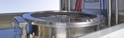
Perfectly meeting this need for a tight wavelength distribution, while exceling in productivity and minimising production costs, is the Aixtron AIX G5+ system in a multi-wafer, 5à—200 mm batch configuration.
Several key technologies contribute to the high yields realised with this reactor. On-wafer yield benefits from: the inherent rotational symmetry of deposition; an optimized RF heater design; and excellent tunability of the distribution of growth species in the gas phase.
Using silicon rather than sapphire is another virtue, because its higher thermal conductivity reduces wafer bow, which in turn decreases the temperature gradient through the wafer and the deposited epitaxial structure. As each wafer's temperature can be controlled to the target set-point, it is possible to realise the overall uniformity requirements for WLCSP (see Figure 3).

Figure 3. The wavelength uniformity for GaN-on-silicon (GoSi) is significantly superior to that of GaN-on-sapphire (GoSap), despite the doubling of wafer diameter to 200 mm.
Another strength of the AIX G5+ is its thermally activated chemical reactor reset. This guarantees the same growth conditions from one run to the next, and prevents silicon wafer edge damage resulting from gallium meltback, and minimizes yield loss through particles and defects (see Figure 4).
Although the benefits of low-cost LEDs produced on large-diameter silicon wafers are compelling, these devices are yet to have an impact in the lighting market. That's because the quality of the GaN films that are grown on silicon is below what is ideal, hampering the device's efficiency and reliability.
Growing high-quality GaN epilayers on silicon is not easy because there is a significant lattice mismatch between the two materials, and a difference in thermal expansion coefficient of nearly 50 percent. These differences can cause crystalline defects, such as dislocations and cracks, that impair efficiency and reliability and ultimately lead to low yield and increased cost.
Cracks, which occur in the GaN epilayer above a certain stress threshold, tend to originate at the wafer edge, where the stress during and after growth is greatest. However, these cracks can propagate further into the centre of the wafer, significantly lowering yield.
Threading dislocations, the other common imperfection associated with GaN-on-silicon epiwafers, appear during the growth, due to the 17 percent lattice mismatch between the two materials. Dislocations can be reduced with strain compensation layers, also known as buffer layers. However, even with this approach, the typical dislocation density of a GaN layer that is grown on silicon is two-to-three times that grown on sapphire. The dislocations hamper sales of GaN-on-silicon LEDs, because they drive down device efficiency, introduce reliability issues and may be the origin of catastrophic failures, due to electrostatic discharge.
By optimising the buffer layers of our LED structures that are grown on 200 mm silicon, we can produce crack-free material with a dislocation density of typically just 3 à— 108 cm-2. The proportion of the wafer that is good enough for chip production is very high (see Figure 4).
One of the biggest advantages of solid-state lighting, compared to incandescent and fluorescent lighting, is the longer lifetime of the source. Although those buying LED bulbs have to pay more than they would do for the alternatives, they have to fork out for them less often, and they are rewarded with lower electricity bills.
Given the longer lifetime of solid-state lighting, it is not surprising that the designers of light bulbs are concerned with the defect density in GaN-on-silicon epilayers. In general, researchers studying catastrophic failure and degradation mechanisms in solid-state lighting have found that failure of the module is more likely than that of the device.

Figure 4. The wafer defect and LED pass/fail map shows the very high quality of epiwafers that may be produced by the Aixtron AIX G5+.
The good news is that our studies with GaN-on-silicon LEDs confirm this view, with thousands of hours of reliability testing revealing that with our strain-managed process, silicon substrates have little to no impact on device reliability compared to sapphire substrates. The degradation characteristics of both types of LED are very similar (see Figure 5 for the device test results).

Figure 5. Samsung's GaN-on-silicon LEDs have a high degree of robustness to electrostatic damage, and their output shows a modest decline over many hours of operation. Note that 25,000 hours corresponds to about 3 years of continual use
Diminished droop
The performance of all forms of GaN LED is held back by droop, a decline in device efficiency at higher drive currents. However, the reduction in performance caused by thermal droop in our LEDs is only about half of that for devices grown on sapphire (see Figure 6). A lower thermal droop is a very valuable attribute, because most mid- to high-power devices operate way beyond room temperature, and it is the lumen-per-dollar that they produce at an elevated temperature that is the best measure of their bang-per-buck. Note that the exact physical mechanism for thermal droop is still under investigation, but it is known that some processes, such as carrier overflow, are stronger at elevated temperatures.
To determine a device's performance in a particular application, it is helpful to measure the junction temperature directly. By making these measurements, we have found that devices grown on silicon run about 20 ËšC cooler than equivalents on sapphire. (We determined this by first extracting the thermal coefficient, which can be measured by applying a low amplitude pulse current as a function of precisely controlled ambient temperature, and then considering the change in forward voltage with temperature "“ in our case the shift in forward voltage at a 350 mA drive current for temperatures from 25 ËšC to 85 ËšC). The lower junction temperature is beneficial, because it trims costs. If the junction temperature is higher, then better and more expensive heat sinks and cooling systems are needed to prevent chip and package degradation.

Figure 6. The external quantum efficiency (EQE) of the GaN-on-silicon (GoSi) LED is very similar to that of GaN-on-Sapphire (GoSap) at 25ËšC, but better at 85ËšC, a typical operating temperature.
The higher levels of strain that are present in GaN layers grown on silicon, rather than sapphire, are viewed as undesirable, because they can impair crystal quality. But that's not a balanced view, as this silicon foundation increases radiative recombination. When GaN is grown on sapphire, there is a compressive strain in the GaN epilayers that results in an in-built piezoelectric field within the quantum wells "“ this occurs through the rearrangement of electronic states in the crystalline structure at the GaN/InGaN interface. This field pulls apart electrons and holes in the quantum wells, reducing the overlap of these wavefunctions and ultimately the radiative efficiency.
When GaN epilayers are grown on silicon, the situation is markedly different. A relatively tensile strain is forced upon the active region, due to the difference in thermal expansion coefficients, and this offsets the piezoelectric field. A reduction in the electric field results, which increases electron-hole wave-function overlap and radiative efficiency.
In addition to the increase in radiative efficiency, the reduction in the electric field strength propels emission to longer wavelengths. Consequently, if the thickness of the wells is maintained, less indium is needed to reach the same wavelength. This is great news, because a reduction in indium content allows growth at higher temperatures, improving crystal quality.
Another encouraging characteristic of our devices is their low thermal droop "“ it is 73 percent lower than that of equivalent WLCSP LEDs grown on sapphire. This superiority underlines the superb crystalline quality of our GaN-on-silicon epilayers. In these devices, thermal degradation in the active region will be less than that for sapphire-based variants, correlating to a more gradual performance degradation and a longer lifetime. As solid-state lighting products are expected to exceed 50,000 hours of operation, this could be a tremendous benefit over time.
In future, it may be possible for LEDs grown on silicon to outperform their more conventional cousins. Such devices would be very promising, given that silicon is well suited to WLCSP. For example, it is easy to remove silicon substrates from GaN epilayers, and it is relatively straightforward to trim the thickness of GaN, which cuts efficiency losses due to absorption of photons within the LED chip. What's more, it is not that challenging to texture the GaN or phosphor surface at the wafer level, to maximize photon extraction efficiency. And efficiencies can be driven up even higher by implementing novel package-level designs, such as multi-layer, multi-colour phosphor coatings.
Based on our work so far, we have an optimistic outlook for the future of the GaN-on-silicon LED. Combining our WLCSP technology with the growth of GaN-on-silicon epiwafers in an AIX G5+ system, we have been able to produce highly efficient LEDs that are on a par with those based on sapphire. We are now commercialising these devices, and we expect them to take a significant share of the LED market. This share could grow if optimisation of these devices allows them to outperform their conventional counterparts, or they are adapted to target other markets. By shrinking their dimensions, micro-LEDs could be produced for next-generation display technology. While sapphire may be the substrate of today, the future surely lies with silicon.


