
LEDs: The compelling case for GaN-on-silicon
BY BURKHARD SLISCHKA FROM ALLOS SEMICONDUCTORS
Many believe that the chance has gone for GaN-on-silicon to play a major role in the LED industry. They argue that GaN-on-silicon technology has taken too long to mature, and the momentum lies with LEDs on sapphire, which have costs that have fallen throughout the last decade.
However, a few firms are swimming against this tide. They include the Korean electronics giant Samsung, which in an article in last month's issue of this magazine highlighted that by combining 200 mm GaN-on-silicon epiwafers with wafer-level, chip-scale packaging it is able to produce high-quality LEDs with a staggering 60 percent lower cost. Samsung concludes that the future of LED making "surely lies with silicon".
So is Samsung a visionary, leading high-volume manufacturer of a disruptive, low-cost technology that other chipmakers are overlooking? Or is the Korean outfit misguided, and soon to be dogged by high costs and persistent low yields?
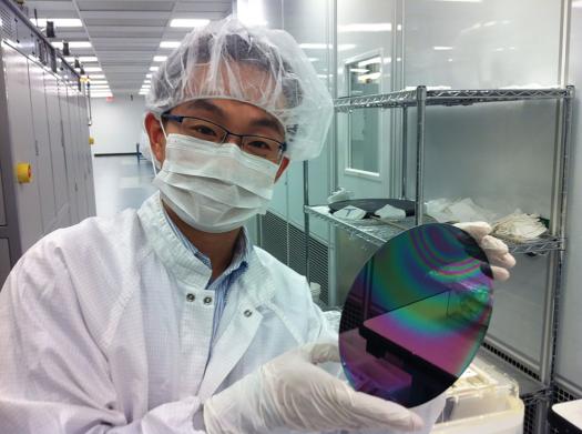
During the last decade, the promise of lower costs, resulting from bigger, cheaper wafers has been the primary driver behind GaN-on-silicon LED development. But it has been tough to turn this dream into a reality, because it is not easy to grow good-quality epiwafers and use them to make high-performance LEDs.
What makes Samsung special is that it has combined three crucial building blocks: access to the low processing cost of silicon lines, which is enabled by good GaN quality and 200 mm epiwafers designed for manufacturability; the use of thin-film LED chips, which become much easier to make when using silicon substrates rather than sapphire ones; and high-yielding, lower cost wafer-level, chip-scale packaging, which becomes possible only with the superior wavelength homogeneity of GaN-on-silicon epiwafers. It is this combination that allows Samsung to achieve the enormous benefits it claims.
Samsung's skeptics will argue that this approach is flawed. In their minds, there are too many changes associated with switching production to silicon substrates.
To back up this view, they might cite Toshiba's woes. In 2013, it invested a great deal of money in acquiring Bridgelux's GaN-on-silicon technology and then building up its capabilities in Japan and the US. By 2015, when it started sampling GaN-on-silicon LEDs, the plan seemed to be working. Many industry insiders were won over by the unrestrained quality of the chips and the promise of low prices.
But Toshiba appears to have suffered from serious yield issues and to have failed to ship large quantities of GaN-on-silicon LED before it was forced to shut down this part of its business at the end of last year, in the aftermath of its financial scandal.
Although Toshiba's experience highlights the challenges for GaN-on-silicon LEDs, it would be folly to discard this technology. The 60 percent cost savings claimed by Samsung are not exaggerated, according to calculations by our team at Allos Semiconductors. More importantly, we see this not just as a one-time cost reduction but rather as a shift to a fundamentally lower-cost curve. So, with such significant savings up for grabs, shouldn't LED executives allocate more time to consider this, rather than devoting all their energy on delivering a cost reduction of "˜only' 5-10 percent in the next quarter?
It is clear that smaller corporations cannot invest as much in GaN-on-silicon technology as Samsung or Toshiba. And unlike this duo, most of them don't have their own silicon lines. Additionally, not all LED makers are fully vertically integrated. Companies which focus on epitaxy and chip making will have to coordinate with their customers to realize the benefits of wafer-level, chip-scale packaging that Samsung enjoys.
Nevertheless, the challenges of entering GaN-on-silicon LED production are not insurmountable. GaN-on-silicon's potential can be unleashed by engaging with technology and foundry partners. Such smart ways can reduce development and production cost, speed-up time-to-market and limit risk. They are available for all three parts of the LED production process "“ epitaxy, device processing and packaging.
Production of high-quality, low-cost GaN-on-silicon LEDs hinges on hetero-epitaxy. Growing GaN-on-silicon requires specialist expertise, most of all in order to achieve the required crystal quality and wavelength uniformity and to ensure manufacturability on cost-efficient, high-throughput reactors. Complicating matters, patents protect a considerably amount of know-how associated with GaN-on-silicon technology.Companies might be daunted by the challenge of developing a GaN-on-silicon epitaxial process of their own. However, they can license our patented, proprietary GaN-on-silicon technology. We will exchange their buffer for ours and help them integrate it with their light emitting structures. Such projects are typically completed within just twelve weeks allowing customers to focus their development effort on device processing and packaging.

Excellent properties of GaN-on-silicon epiwafers enable high yield and cost savings in device processing and packaging.
For device processing, switching from sapphire to silicon is not just a matter of transferring to large diameter processing equipment and the need to introduce more complex thin-film production processes. The biggest challenge is having access to a 200 mm processing line. Here we see that partnering with a low-cost, high-volume silicon foundry is an attractive option: it offers a new business opportunity for the foundry, and equips the LED maker with a more variable cost structure, while at the same time reducing its capital expenditure.
Wafer-level, chip-scale packaging is a technology that many LED companies have investigated with sapphire substrates, but insufficient uniformity has prevented implementation in the manufacturing process. As Samsung has shown, this situation can change when the process is performed on uniform, 200 mm GaN-on-silicon epiwafers. Companies that are lagging behind in the development of wafer-level, chip-scale packaging technology could turn to specialized technology advisers or tap into the expertise of the packaging foundries from the IC industry.
With key technologies now in place, Samsung will refine its processes as it ramps up production. Rivals with underutilized sapphire-based capacity and a lack of silicon line experience may look on in awe, fearing that the barriers to entry are too high. But rather than being paralyzed by the challenges of bringing GaN-on-silicon LEDs to market, Samsung's actions should be viewed as a wake-up call for other LED chipmakers. The cost-saving potential of the technology is huge and there are smart ways to tackle the challenges.


