
Veeco: Taking red, orange and yellow LEDs and optoelectronics to the next level
A: The markets are: red, orange and yellow LEDs, which are primarily driven by displays and signage, automotive, and some of the lighting market; and the solar cell market, which is triple-junction solar cells that are mostly used in space applications. The other market that is up and coming is in optoelectronics "“ it is the laser telecom market.
Q: Currently there is a great deal of interest in wearable applications. Are your customers optimistic about this? And are there specific products or product applications that you, or they, are particularly excited about?A: Wearables is an interesting area. The way I see wearables is not just from a display perspective. There are a variety of wearables and the primary driver that we can see enabling the future is very similar to one of the market segments that I just talked about, the optoelectronics segment. A bunch of sensors are going to get integrated into these wearables, enabling more accurate biometric sensing and gesture recognition. That's where you will need both arsenic/phosphide-based devices and GaN-based devices.
From a light-generation perspective, we don't see a huge market for wearables, because the number of LEDs in a wearable is very small.
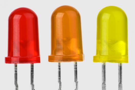
Q: Primary markets for red, orange and yellow LEDs include outdoor displays and signage. Are the end markets growing, in terms of volumes and revenue?A: Typically, we are seeing close to a 10 percent compound annual growth rate in the red, orange, yellow (ROY) market. It is primarily driven by, as you say, displays and signage, automotive, and some lighting-based devices.
In terms of LED unit count, the ROY market is probably a one-to-eight to a one-to-ten ratio of the blue LED market.
Q: The manufacture of red, orange and yellow LEDs dates back far further than that of their blue cousins, which are now used extensively in general lighting. How does the production of these two types of devices compare, in terms of the requirements to deliver a competitive product?A: For a competitive product, you have to look at how to develop a certain level of thickness uniformity.
Red, orange and yellow LEDs have a Distributed Bragg Reflector (DBR) beneath the active region. The thickness uniformity of these layers is extremely critical to meeting the right wavelength of light. What we pay attention to is the DBR uniformity and the repeatability of those layers.
In a blue LED, you use a multi-quantum well (MQW), and if that uniformity shifts you will have a big binning issue. In the GaN-based LED, we pay attention to the wavelength uniformity and thickness uniformity of the MQW layers, primarily.
Q: Judged in terms of profit margins, is it better to be making blue LEDs, or red, orange and yellow variants?A: It depends. The reason why I say it depends is that even in the red, orange and yellow, there is one segment, automotive, that's a pretty high-margin, high-revenue segment for our customers. The requirements there are very much more demanding, in terms of reliability and brightness.
In very low-end toys, and very low-end signage and displays, profit margins are razor thin. Comparing the blue LED versus the red LED, I think profit margins are very similar if you are just competing in the low-end to mid-end range.
If you go to tier one manufacturers, like Nichia, Lumileds and Osram, they are going into more speciality lighting and automotive. Their profit margins are very different.
Q: How does the K475i build on your previous tool for arsenide and phosphide growth, the K475?A: Our core technology is the TurboDisc platform. In the GaN space, we had a K465. We then developed a uniform flow flange, based on TurboDisc technology, and launched the K465i. From then on we have scaled to MaxBright and EPIK, and gained market share leadership.
We are doing exactly the same with arsenides/phosphides. Our core system is the K475. The K475i is fundamentally a much better high-uniformity, highly repeatable tool.
Q: What are the pros and cons of the K475i compared to rival tools for the growth of arsenides and phosphides?A: The fundamental advantage is a strong TurboDisc technology. Repeatability of the uniformity is very, very high, and because of TurboDisc technology "“ it is a laminar flow "“ the time between preventative maintenance (PM) is very long. What this means is that you can go for long campaigns, with highly repeatable results, within the wafer, wafer-to-wafer and run-to-run, for every batch of wafers that you put in and take out.
Another advantage of the TurboDisc technology is inherently less defects and particles, for better device performance. So you don't need to clean every run or every few runs "“ you can go through hundreds of runs without any cleaning inside the chamber. That's a core advantage that is fundamental to the new applications that are coming along. But even with ROY, when LEDs go into higher-end automotive, particle performance is really critical.
Q: You claim that the new K475i system has been able to reduce the cost-per-wafer by 20 percent. That's a substantial margin. How have you achieved this?A: It's based on the advantages of longer campaigns, longer intervals between PMs, and much higher uniformity. You not only increase productivity "“ you add yield. When you combine those two, you get to a 15 to 20 percent range of cost-of-ownership benefits (see "Calculating cost-of-ownership for MOCVD capital equipment" for more details).
Q: The K475i can be configured as a 15 x 4-inch tool, or a 7 x 6-inch tool. What do you expect to be the most common configuration?A: Most of the tier one customers are using this in 6-inch, and most of the rest of the world is in 4-inch.
Q: To what extent is the K475i future-proof?A: The K-platform was built future-proof, which means with future upgradability in mind. The K475 can be upgraded to the K475i. Beyond the K475i, if we have to improve certain parameters inside the tool to improve performance, we would take a very close look at it. We protect the initial investment of the capital for the customer. It's very important.
Q: You have worked with Changelight on the development of the K475i. What are the benefits of working with this LED maker when developing the reactor?A: The reactor and the core technology we developed ourselves. I would say that's the fundamental core IP for Veeco.
Why we work with Changelight, and why Changelight has been very helpful, is that they were our beta-partner in qualifying the K475i. They used the tool from the initial process runs all the way to chip-level data, to prove that this reactor is equal or better than their current system. It's also very important to validate customer qualification and acceptance. Veeco has a strong track record of meeting demo specifications and obtaining positive customer endorsements.
Q: China is accounting for an increasing proportion of LED chip production. Is this the primary market for the K475i?A: It is one of the primary markets for the K475i. China has a lot of ROY LED production by unit volume, but there is also a pretty healthy volume of production of ROY LEDs/arsenide/phosphide devices outside China. Our expectation for this tool is that it will go into multiple applications beyond ROY LEDs and help us to compete very effectively against the competition, having made this investment in furthering the product roadmap.
Q: The K475i can be used to make lasers, solar cells, pHEMTs and HBTs. Do you expect to sell many tools to the producers of these devices?A: In each of these segments, the market trends are different. If you take lasers or solar cells, versus pHEMTs and HBTs, they are in different parts of the market adoption curve. pHEMTs and HBTs are a lot more mature from a market perspective, but one of the growing segments that we see, and what we call the opto market, is the laser market. Talking to our customers, it has primarily been driven by the megatrend of cloud computing, data storage and big data, driving the need for higher-speed communication. People are downloading a lot of videos and data, so there is a lot of bandwidth that is needed to keep up, because data transfer is going higher and higher. Communication lines are moving from copper to optical, which drives the need for lasers.
Q: What does that mean from the perspective of Veeco?A: We expect to sell, over the next few years, several tools into this segment. At this moment we are also trying to map what this growth trend means in the long-term "“ and how big the market can be.
Q: Earlier this year you teamed up with imec, starting work on a project to accelerate the development of GaN-on-silicon power devices, using your Propel Power GaN System. What progress have you made to date, and what are your next targets?A: The goal is to further validate with industrial partners, through the imec consortium, that the Propel system, which is our single-wafer-based MOCVD technology, delivers highly cost-effective GaN-based power devices.
The Propel Power GaN System is akin to what has happened in the semiconductor industry. Early in the semiconductor industry batch systems were the tools of choice, and as the node size got smaller and smaller, companies migrated from batch tools to single-wafer tools, which gave significantly superior on-wafer performance. This is fundamental to the device, even though it was "˜expensive'. The device values trumped, and enabled customers to go to the next level.
We believe the same thing is going to happen in the power electronics space, on the GaN-based power devices. That's the fundamental reason we developed the Propel technology "“ to further enable the market to cross over the chasm.
Q: How big do you think the GaN-on-silicon power market could be?A: We believe the GaN-on-silicon power market is going to have strong play in the sub 650 V operating range. One of the things that we see "“ that is creating a need in the consumer space "“ is wireless charging. Large companies are trying to create wireless charging devices, so you don't always need to connect your device, or even place it on a mat.
We see more steady growth and steady penetration for the GaN-on-silicon power market. What the market research guys say is the end market is going to be somewhere between $300 million and $500 million in the next five years. But my personal belief is that there will be an inflection point, and when it happens, it can be a lot bigger than people predicted.
A: For arsenide/phosphide-based epitaxy for ROY LEDs or lasers, from an epitaxial perspective, it is primarily flow uniformity that we have to work on. So long as you get your flow uniformity, then by design you will get the uniformity of the DBR layers, which means that your yield will be high. So the batch works perfectly.
When it gets to the next level of complexity, you need to have very good flow uniformity and extremely good thermal uniformity, so you probably want to go towards a single-wafer platform for GaN-based devices. It is the same argument for blue LEDs, for the mid-power range. The EPIK 700 multi-wafer platform is the flagship, and will continue to remain so. If there is a need to get extremely tight wafer uniformity levels, then probably the industry will move to single wafer.
 At the heart of the K475i system is Veeco's production proven TurboDisc reactor technology
A: We believe we have all the bases covered. We have three platforms: we have an EPIK platform for GaN-based devices for blue LEDs; we have a platform K475i, which is arsenides/phosphides-based; and we have a Propel platform "“ power is the first segment we will address, and we believe that there are future segments that we can address using Propel.
You will see more products coming out of the Propel platform that are single-wafer based. Epitaxy is like lithography, you've got to get it right before you can get your device right.

Veeco introduced the TurboDisc K475i As/P MOCVD System to meet demand for red, orange, and yellow (ROY) LEDs for displays, signage and automotive markets as well as for solar and optoelectronic manufacturing.
Calculating cost-of-ownership for MOCVD capital equipmentLED manufacturers are constantly looking for ways to improve profitability. One way to do this is to trim manufacturing costs by reducing expenditure on capital equipment. However, it is folly to select equipment solely on its price. Instead, one must balance the initial purchase and installation costs with other critical factors that determine the cost of ownership. Over the life of an MOCVD system, throughput rates, equipment reliability and yield have a greater impact on cost-of-ownership than initial purchase costs.
To make an informed decision when purchasing an MOCVD system, the lifetime cost-of-ownership must be considered. This is the same as the cost per wafer.
Cost per wafer = total cost (fixed costs + varaiable costs)
throughput x utilization x yield
In this equation fixed costs include purchase, installation and facilities costs that are normally amortized over the life of the equipment; variable costs include materials, labour repair, consumables, floor rent, utility and overhead expenses incurred during equipment operation; throughput is the time needed to meet a process requirement, such as depositing a nominal film thickness; utilization is the ratio of production time to total available time; and yield is a measure of defects and the uniformity of key quality parameters on the wafer. In the case of an LED, this would include peak wavelength and forward voltage.
There are five key benefits associated with using a cost-of-ownership model:
- It creates a common standard for LED manufacturers to objectively scrutinize operations
- It provides an objective analysis method for evaluating decisions
- It offers a clear tool estimate for the cost of ownership
- Equipment suppliers can use common decision-making elements to make better-informed decisions on future product offerings
- It helps to foster greater cooperation between equipment suppliers and users, to provide input parameters and data that will benefit the industry


