

EYEQ Lab reveals 200mm SiC wafer
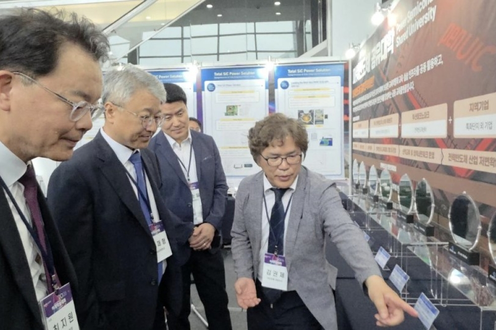
Last month, EYEQ Lab, a Korean power semiconductor company, unveiled Korea's first mass-produced 8-inch (200 mm) SiC power semiconductor wafer at the 2026 Korean Institute of Electrical and Electronic Material Engineers (KEMS 2026), held from June 24–26 at BEXCO in Busan.
The company was exhibiting its production-ready 8-inch SiC wafers, manufactured at its recently established 8-inch SiC dedicated fabrication facility in Busan, marking a milestone for Korea's power semiconductor industry.
Alongside the wafer exhibit, EYEQ Lab exhibited a range of application products powered by its proprietary Q-Device SiC technology, including a 65W SiC quick charger, a high-efficiency SiC power module, and Intelligent Power Modules (IPMs) for industrial and consumer applications.
Last year, EYEQ Lab completed Korea's first dedicated 8-inch SiC fabrication facility within the Busan Power Semiconductor Materials, Components and Equipment Cluster. The company has since focused on process stabilisation and yield optimisation and is now advancing toward full-scale mass production.
"This exhibition represents the first official public presentation of Korea's first mass-produced 8-inch SiC wafers," said an EYEQ Lab spokesperson. "Through our Q-Device-based power semiconductor solutions, we aim to enhance the competitiveness of Korea's power semiconductor industry while expanding our presence in the global market."
The company's 8-inch SiC fabrication facility in Jangan-eup, Gijang-gun, Busan, has an annual production capacity of up to 30,000 wafers, and EYEQ Lab says it is expanding commercial supply to customers worldwide.



