

The QPCSEL: a new approach to building lasers
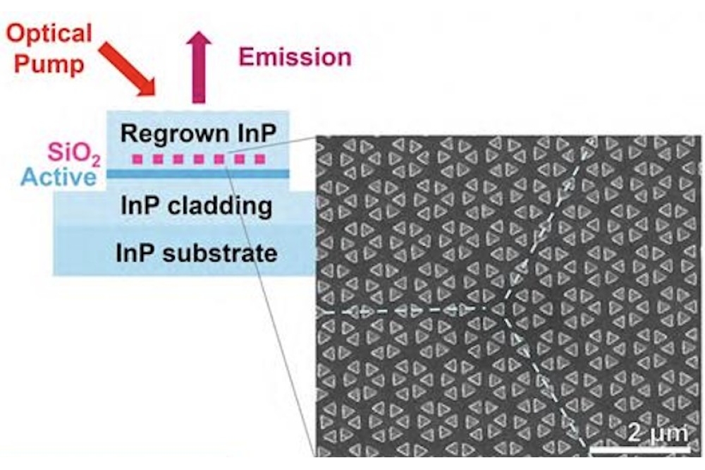
Over the past two decades, photonic-crystal surface-emitting lasers (PCSELs) have shown promise as a type of advanced semiconductor laser. Typically, PCSELs are made with photonic crystal patterns, which repeat across the area of the device.
Now new research published in Applied Physics Letters by a group at the Grainger College of Engineering at the University of Illinois Urbana-Champaign has demonstrated a quasi-periodic QPCSEL.
Kent Choquette's group in the lab of electrical and computer engineering, used their buried dielectric platform to create what they describe as a tuneable and more reliable semiconductor laser.
One challenge for the PCSEL field has been its reliance on geometry-dependent device fabrication. While a photonic crystal pattern can be optimised for certain properties, researchers have limited options for fabricating new devices with a wide variety of pattern shapes and sizes. Wanting to introduce a more versatile method, graduate student Erin Raftery began with a goal: to make a periodic structure non-periodic.
Drawing inspiration from other work on topologically-protected — or non-repeating — patterns, Raftery integrated a similar patterning method with her group’s existing buried dielectric platform, which they first demonstrated in 2025. While most layered semiconductor materials are fabricated by etching tiny holes vertically through the device, Raftery etched a silicon dioxide layer which was then covered by epitaxial semiconductor, embedding it in the device. The resultant partially periodic structure lased successfully at room temperature as is described in the paper 'Buried dielectric quasi-photonic-crystal surface-emitting lasers'.
“We’ve demonstrated that we can have a non-periodic pattern and more flexibility to tune it,” Raftery said. “It’s a different way of engineering the refractive index variation to get the properties we want from our lasers.”
In its current iteration, the platform’s primary advantage lies in the versatility and uniformity that the buried dielectric photonic crystal pattern possesses.
“Right now, you can only grow one kind of structure at a time, whereas we can mix and match on the same substrate,” Choquette said. “This could allow us to build more reliable, better-performing lasers.”
Now, the Illinois Grainger engineers are turning their attention to making a more practical semiconductor laser. In the future, they hope to demonstrate an electrically-injected diode — a more challenging pursuit with commercial implications.
“We’ve demonstrated the physics,” Choquette said. “Now we need to demonstrate a practical device.”



