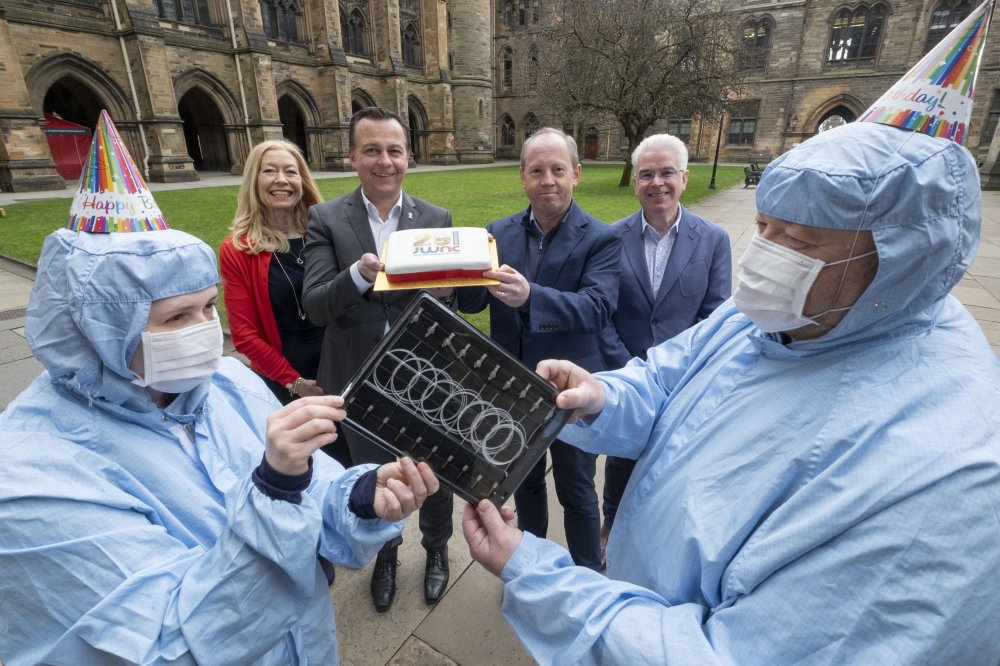
Scientists develop three-in-one diode
PN junction diodes are the underpinning of modern optoelectronic systems. But, typically, they perform only a single task. To process complex visual signals, optical imaging systems often rely on the introduction of a third electrode or integrating diodes with external logic circuits.
But these architectures increase hardware complexity and bring von Neumann issues — the physical separation of sensing, memory, and computing—leading to larger areas and increased power consumption. There is a lack of a compact, single-device solution.
Now, in a study titled 'A single diode with integrated photosensing, memory and processing for neuromorphic image sensors' published in Nature Electronics, a research team led by SUN Haiding from the University of Science and Technology of China of the Chinese Academy of Sciences, along with the collaborators from domestic and foreign universities, have developed a multifunctional photodiode architecture.
They appraoch, they say, provides a hardware solution for low-power neuromorphic visual cameras with integrated sensing, memory, and computing, breaking through the traditional semiconductor physical limit of unidirectional conductivity.
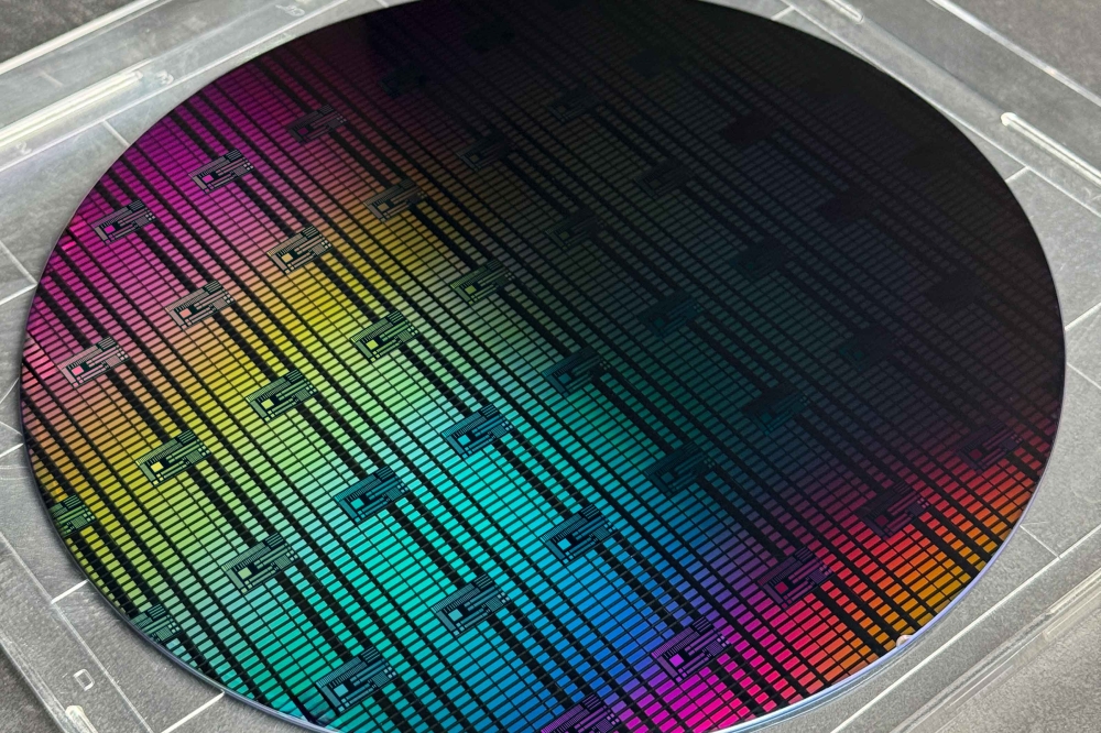
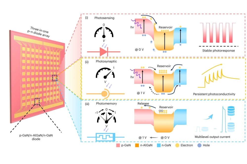
The new PN junction design is based on energy band engineering. The team constructed high-crystal-quality vertical GaN-based PN junction diode arrays on conductive silicon substrates. By inserting a wide-bandgap n-AlGaN layer into the GaN-based PN junction, they formed a localised 'charge storage layer' internally via energy band bending. This embedded structure endowed the device with unique charge trapping and releasing capabilities, enabling arbitrarily mode switch through simple external bias voltages without altering the device structure.
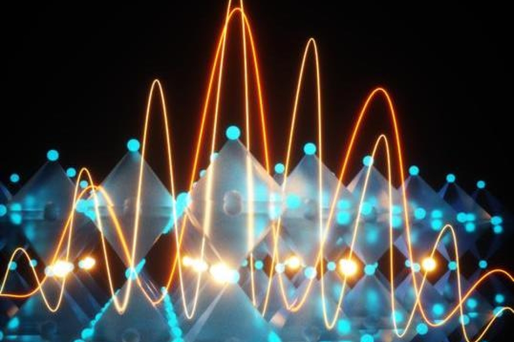
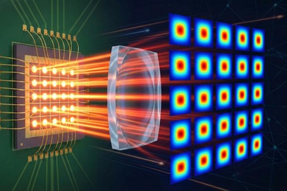
The team demonstrated that a single device could exhibit three independent and freely switchable working modes: photosensing, photosynapse, and photomemory. Under zero bias, the device exhibited stable self-driven photosensing characteristics for real-time image sensing. Under a constant bias, it demonstrated photosynaptic behaviour modulated by pulse frequencies. Under pulsed bias operation, it achieved multi-state optical memory capacity. This voltage-modulated multi-mode functionality paves the way for neuromorphic smart sensing cameras capable of real-time sensing alongside edge image de-noising and classification.
A neuromorphic visual camera demonstration system using a 10×10 crossbar array was shown to accomplish the entire image processing workflow in situ solely by adjusting the applied bias voltage. By exploiting the difference in electron release rates between low-frequency noise and high-frequency image signals, the system achieved hardware-level image de-noising. It then classified the processed images by functioning as an artificial neural network. This hardware-level intervention significantly boosted image recognition accuracy from below 60 percent before de-noising to over 95 percent.