KAIST team develops selective transfer printing for MicroLEDs
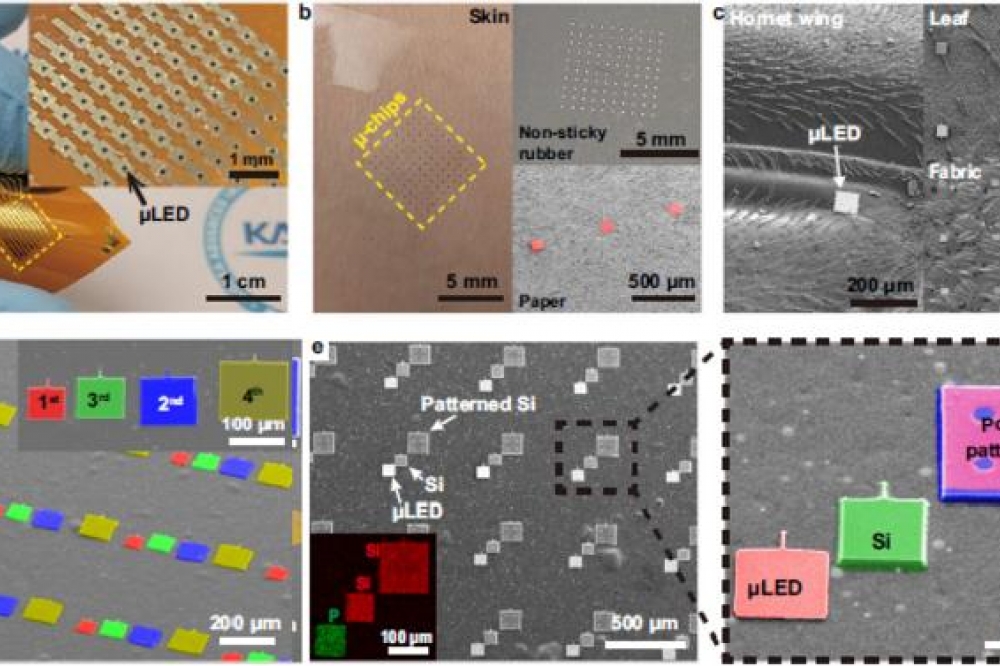
New approach can transfer a large number of microLED chips by adjusting micro-vacuum suction force
To commercialise microLEDs, transfer printing technology is essential for rearranging microLED dies from a growth substrate onto the final substrate. However, current methods still have many challenges such as the need for additional adhesives, misalignment, low transfer yield, and chip damage.
The research team of Keon Jae Lee, a professor at KAIST (the Korea advanced Institute of Science and technology), has developed a micro-vacuum assisted selective transfer printing (µVAST) technology to transfer a large number of microLED chips by adjusting the micro-vacuum suction force.
The paper describing the work 'Universal selective transfer printing via micro-vacuum force' was published in Nature Communications on November 26th, 2023.
The key technology relies on a laser-induced etching (LIE) method for forming 20 μm-sized micro-hole arrays with a high aspect ratio on glass substrates at fabrication speed of up to 7,000 holes per second. The LIE-drilled glass is connected to the vacuum channels, controlling the micro-vacuum force at desired hole arrays to selectively pick up and release the microLEDs.
According to the scientists, the micro-vacuum assisted transfer printing accomplishes a higher adhesion switchability compared to previous transfer methods, enabling the assembly of micro-sized semiconductors with various heterogeneous materials, sizes, shapes, and thicknesses onto arbitrary substrates with high transfer yields.
Keon Jae Lee said: “The micro-vacuum assisted transfer provides an interesting tool for large-scale, selective integration of microscale high-performance inorganic semiconductors. Currently, we are investigating the transfer printing of commercial microLED chips with an ejector system for commercialising next-generation displays (Large screen TVs, flexible/stretchable devices) and wearable phototherapy patches.”