Loading...
News Article

CRAIC launches 5D spectral surface mapping tool

News
Multi-modal spectral techniques and new mapping algorithms allow researchers to unravel the complexities of diverse materials

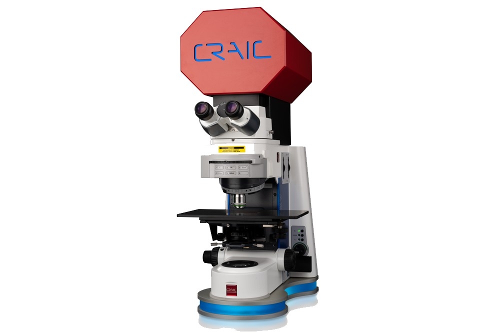
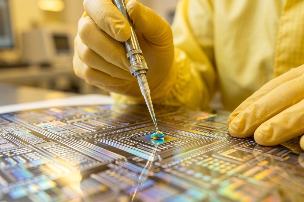
CRAIC Technologies, a Californian provider of scientific instrumentation, has launched its 5D Spectral Surface Mapping tool for analysing the composition, morphology, and behaviour of materials at the micro and nanoscale.

Spectral mapping, a technique combining spectroscopy and microscopy over surfaces, allows researchers to visualise and analyse the spatial distribution of chemical and structural properties within samples with high detail and precision.

"The introduction of our 5D Spectral Surface Mapping solution marks a significant milestone in the field of materials science and microscale spectroscopy," said Paul Martin, president of CRAIC Technologies.

"By integrating high-performance UV-Visible-NIR, Raman and Photoluminescence microspectroscopy systems with sophisticated spectral analysis and mapping algorithms, we are enabling researchers to unravel the complexities of diverse materials with unprecedented clarity, accuracy, and efficiency."

The 5D Spectral Surface Mapping tool's spectral mapping algorithms facilitate the acquisition of spatially resolved spectral data across samples, allowing researchers to correlate chemical and structural information with sample morphology and composition.

The support of multi-modal spectral techniques, including UV-visible-NIR, fluorescence, photoluminescence, Raman and thin film thickness, providing researchers with versatile spectral imaging options for a wide range of sample types and research objectives.

Intuitive software interface and data visualisation tools are designed to streamline data acquisition, analysis, and interpretation, enabling researchers to extract meaningful insights from complex spectral datasets with ease, according to CRAIC.

Tariff uncertainty weighs on displays
Flexible perovskite/CIGS tech reaches 23.64% efficiency
IQE and X-FAB sign GaN power collaboration
Riber reports solid growth in sales and earnings
How to make green ZnSeTe QD-LEDs brighter
Korean team makes novel flexible ammonia sensor
Optimising green LEDs for near-eye applications
MoD to put £200m into UK compound semi fab
EU invests €15M to help firms use photonics
ST and Innoscience sign GaN deal
Lumentum shows InP advances at OFC
A step towards higher DUV LED efficiency
Quantum Science achieves ISO 9001:2015 certification
Ascent wins order for power-beaming module
Navitas Partners with Great Wall for 400V-DC power
SemiQ supplies SiC MOSFET modules for EV battery cell cyclers
Coherent and Keysight collaborate on 200G/lane multimode VCSEL tech
Lumentum and Marvell exhibit integrated 450G optical interface
Marktech announces new MWIR LEDS
Imec identifies stable range for GaN MISHEMTs in RF PAs
Polar Light completes $3.4m funding round
Lynred launches advanced thermal imaging modules
Altum RF expands Sydney design centre
Sivers announces partnership with O-Net
Ayar Labs unveils first UCIe optical chiplet
Aixtron delivers InP tool to Nokia
WHU-USTC team demo novel GaN chip temperature monitoring
Phlux lands £9m to take InGaAs sensors to next level
4-inch gallium oxide facility established in Swansea
Mazda and Rohm collaborate on automotive GaN
University of South Carolina chooses MOCVD tool from TNSC
Wolfspeed appoints new CEO amidst funding crisis
×
Search the news archive

To close this popup you can press escape or click the close icon.
Logo
x
Logo
×
Register - Step 1

You may choose to subscribe to the Compound Semiconductor Magazine, the Compound Semiconductor Newsletter, or both. You may also request additional information if required, before submitting your application.


Please subscribe me to:


You chose the industry type of "Other"

Please enter the industry that you work in:
 
x
Adblocker Detected
Please consider unblocking adverts on this website