Optimising green LEDs for near-eye applications
A common approach for producing commercial, high-current LEDs involves the inclusion of pre-well layers – these superlattices, featuring low-indium content layers, are inserted before the active region to aid strain engineering.
However, research by a team from China has shown that removing these pre-layers ensures a better performance for green microLEDs for near-eye applications, as their absence trims piezoelectric polarisation fields in quantum wells and suppresses Auger-Meitner non-radiative recombination.
According to Junyong Kang from Xiamen University, these benefits that come from removing the pre-well layers stem from a reduction in interfacial defects in quantum wells. Minimising these imperfections leads to a significant enhancement in radiative recombination efficiency at low current densities.
“This advancement is critical for near-eye display applications, such as AR/VR/MR,” says Kang, who is keen to emphasise that this structure is not suitable for far more powerful LEDs.
The team from Xiamen University and Xiamen Changelight have demonstrated the success that’s possible with their approach by producing green microLEDs with either six pre-wells, three pre-wells, or the absence of pre-wells, and comparing emission characteristics.
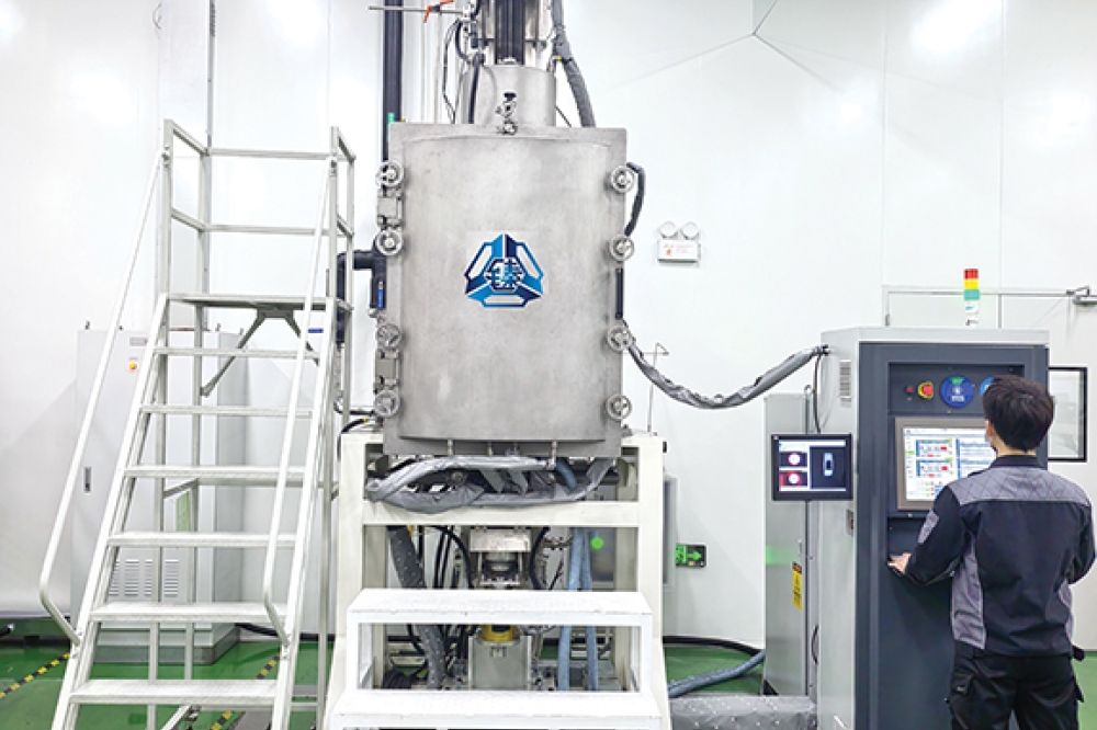
Fabrication of this team’s portfolio of green microLEDs began by taking a patterned sapphire substrate and depositing a 45 nm-thick layer of AlON.
“The aluminium oxynitride buffer layer is realised through a combined process of PVD sputtering and MOCVD epitaxy,” says Kang, who reveals that depositing this layer is less of a challenge than addressing lattice and thermal mismatches with subsequent, GaN-based epilayers. “During growth, precise control of temperature gradients and V/III ratios is required, coupled with in-situ stress monitoring for dynamic compensation.”
After loading this AlON-on-sapphire foundation in an MOCVD chamber, the team added a 4 µm-thick layer of undoped GaN, followed by a 2 µm-thick n-type layer, an active region with three In0.20Ga0.80N quantum wells, a 20 nm-thick AlGaN blocking layer, and a pair of p-doped layers. Variants with pre-wells featured In0.05Ga0.95N superlattices.
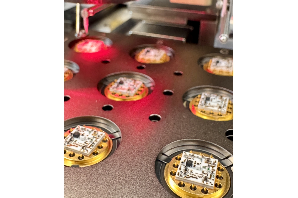
Epiwafers were processed into microLEDs with dimensions of 17 µm by 20 µm, using a number of steps that included adding an ITO transparent conductive layer, employing rapid annealing to create an ohmic contact with p-type GaN, and applying photolithography and plasma etching to expose areas of n-type GaN.
During growth of multiple quantum wells, it is inevitable that defects, which subsequently facilitate the formation of V-pits, are generated at interfaces between quantum wells and adjacent barrier layers. Scanning electron microscopy images of the all three types of epiwafer have confirmed that reducing the number of pre-wells leads to fewer V-pits, thanks to a reduction in the total number of interfaces.
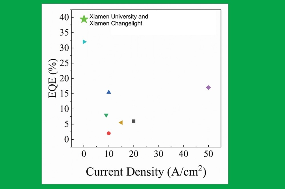
Measurements of external quantum efficiency have revealed maximum values of: 31 percent at 0.3 A cm-2 for the microLED with six pre-wells, 36 percent at 0.12 A cm-2 for the microLED with three pre-wells, and 39 percent at 0.07 A cm-2 for the microLED without any pre-wells. According to the team, an external quantum efficiency of 39 percent is the highest value ever reported.
To understand the variation in external quantum efficiency with different designs of microLED, the team applied the well-known ABC model to the data, to determine coefficients for Shockley-Read-Hall recombination, radiative recombination and Auger-Meitner recombination. Compared to the value of Shockley-Read-Hall recombination for the microLED with no pre-wells, variants with three and six pre-wells had values four and six times higher.
This finding reveals that decreasing the number of pre-wells increases the quality of the multi-quantum wells, improves uniformity and supresses the non-radiative Shockley-Read-Hall recombination that results from defects.
Kang and co-workers are now planning to build on their expertise in defect engineering, strain compensation and carrier transport optimisation in high-indium-content materials. Future efforts will focus on developing red and yellow LEDs based on InGaN that overcome critical epitaxial growth challenges.
Reference
A. Wang et al. Appl. Phys. Express 18 011001 (2025)