Going through the gears with gallium nitride
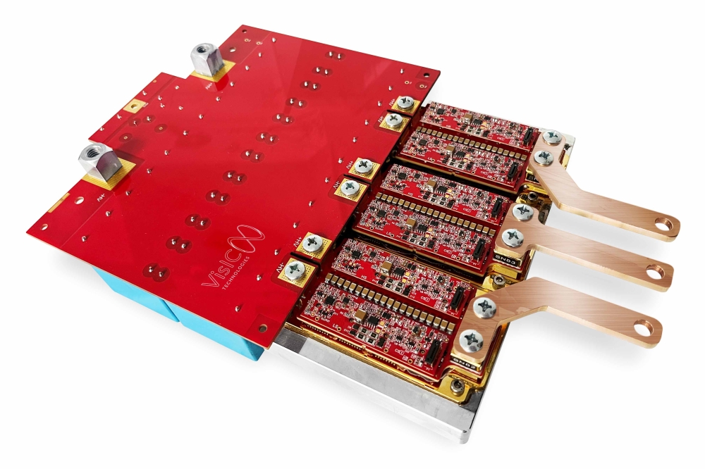
VisIC plans to ramp production of its GaN depletion-mode HEMTs for electric vehicle inverters before the end of this decade.
BY RICHARD STEVENSON, EDITOR, CS MAGAZINE
Designers of electric vehicles are facing a dilemma when selecting the power electronics for their drive trains. To trim the bill of materials, they favour the use of the silicon IGBT. But this transistor fails to offer the efficiency of the pricier SiC MOSFET, which ensures a greater driving range for the automobile, an attribute that has spurred the commercial success of this class of transistor.
Due to these awkward trade-offs, designers of EVs will be enthralled by the tantalising prospect of a power transistor that delivers a performance on par with that of the SiC MOSFET, but for a price comparable with that of the silicon IGBT.
Preparing to offer just that in significant volume within the next few years is the Israeli-based producer of GaN power devices, VisIC Technologies, which is working in partnership with AVL, one of the leading developers, simulators and testers of many forms of green transportation.
“We can really push the boundaries and technology with AVL,” enthuses Dieter Liesabeths, Senior Vice President of Product at VisIC. He says that this partner excels in software knowledge and hardware experience, and will provide great support in the development of highly integrated inverters. “They also have the capability to go to a very high RPM with their motors, up to 30,000 RPM, which is really benefiting the GaN technology.”
In December 2024, VisIC and AVL reported efficiencies for their inverter of 99.67 percent and 99.8 percent at 10 kHz and 5 kHz, respectively. These values for efficiency are said to be up to 0.5 percent higher than those for SiC inverters, an improvement that ensures a trimming of energy loss by more than 60 percent.
The partnership between VisIC and AVL determined these efficiencies by testing their inverter under 400 V, a voltage that’s used in many city-type cars, as well as those made by Tesla.
Despite much interest is moving EVs to 800 V, these results are incredibly relevant, argues Liesabeths: “The majority of cars that will come out in the future will be 400 volts, because these are typical city-cycle cars, which are having smaller batteries.”
For these EVs, most driving is in urban areas, where the typical average speed is around just 25 km hr-1. At these modest speeds, the load condition on the inverter is relatively low, and this drags down the efficiency of inverters with VisIC’s HEMTs to 99.2 percent. However, that’s still better than that for inverters based on SiC operating at higher loads, thanks in part to the vanishingly small switching losses for GaN.
The GaN HEMT also has the upper hand in terms of price, costing about half that of the SiC MOSFET. The GaN HEMT is still about 20 percent more expensive than the silicon IGBT, but if the former were to be produced using 300 mm wafers, cost-parity with silicon might be within reach, thanks to the smaller size of the die.
Note that lower chip costs are a big deal for makers of EVs. “If you can replace silicon carbide, which is around 55 to 60 percent of the cost of the invertor, with gallium nitride, you're cutting your cost almost by half,” says Liesabeths.
In addition, replacing SiC MOSFETs with GaN HEMTs ensures a substantial reduction in carbon footprint, as producing the former involves very high temperatures.
AVL Dyno test setup with a VisIC D3GAN power inverter.
Depletion-mode devices
VisIC differentiates itself from its rivals with a patented D-mode HEMT technology, pairing its depletion-mode GaN transistor in series with a silicon MOSFET. It’s a novel configuration that enables direct driving of the GaN transistor, thereby avoiding losses that come from switching the silicon MOSFET; and it allows control over the slew rate, leading to greater robustness at the system level. What’s more, the company’s D-Mode technology offers a superior dollar-per-amp, as this form of HEMT can be smaller than its enhancement-mode cousin.
Many producers of GaN HEMTs partner with 200 mm foundries, which were in very high demand during the pandemic. However, this constraint has now eased, says Liesabeths, who can't see any difficulties or bottlenecks in the future for GaN. He points out that foundries offering GaN power electronic technologies are increasing their capacity, and those dedicated to silicon are branching out into GaN.
Initially, VisIC partnered with TSMC, which can handle all steps of production, by producing GaN-on-silicon epiwafers and process them into HEMTs. But now VisIC is also starting to investigate an alternative supply chain, involving independent epiwafer specialists, as well as foundries that process this material into devices.
“Working with dedicated epi-partners means that we have better control, and more influence about the design itself,” says Liesabeths. “The quality is the key differentiator here, because controlling epi means controlling how your device is performing.”
Power modules based on ViSIC’s HEMTs are now undergoing full qualification, under the AEC-Q101 and AQG-324 criteria used in the automotive industry to verify reliability.
“We are confident that we are passing this qualification and even exceeding some of the requirements,” says Liesabeths.
Looking ahead, plans for the partnership include developing very high-power inverters, operating in the 300 kW range, and demonstrating variants around 100-120 kW, suitable for city cars. Liesabeths says that accomplishing all of this will show that GaN is viable for “both ends of the spectrum”.
For VisIC, another target is to produce GaN HEMTs for EVs in high-volume by 2028-29. “We are confident that by this time frame, we will see the first cars on the road,” says Liesabeths, who is helping to lay the foundations for this success, via ongoing work with OEMs and tier ones.
If and when the EV industry moves to higher voltages, VisIC is well-prepared with its patented multi-channel devices that can handle up to 3.3 kV.
“We were not utilising [this technology] so far, because we first want to demonstrate a viable solution for 400 volts,” says Liesabeths. But his co-workers are developing 800 V devices for market, slated for release within the next two years.


