WHU-USTC team demo novel GaN chip temperature monitoring
Researchers from Wuhan University (WHU), University of Science and Technology of China (USTC), and China Electronics Product Reliability and Environmental Testing Research Institute (CEPREI) have developed a novel temperature charactersation method for GaN HEMTs.
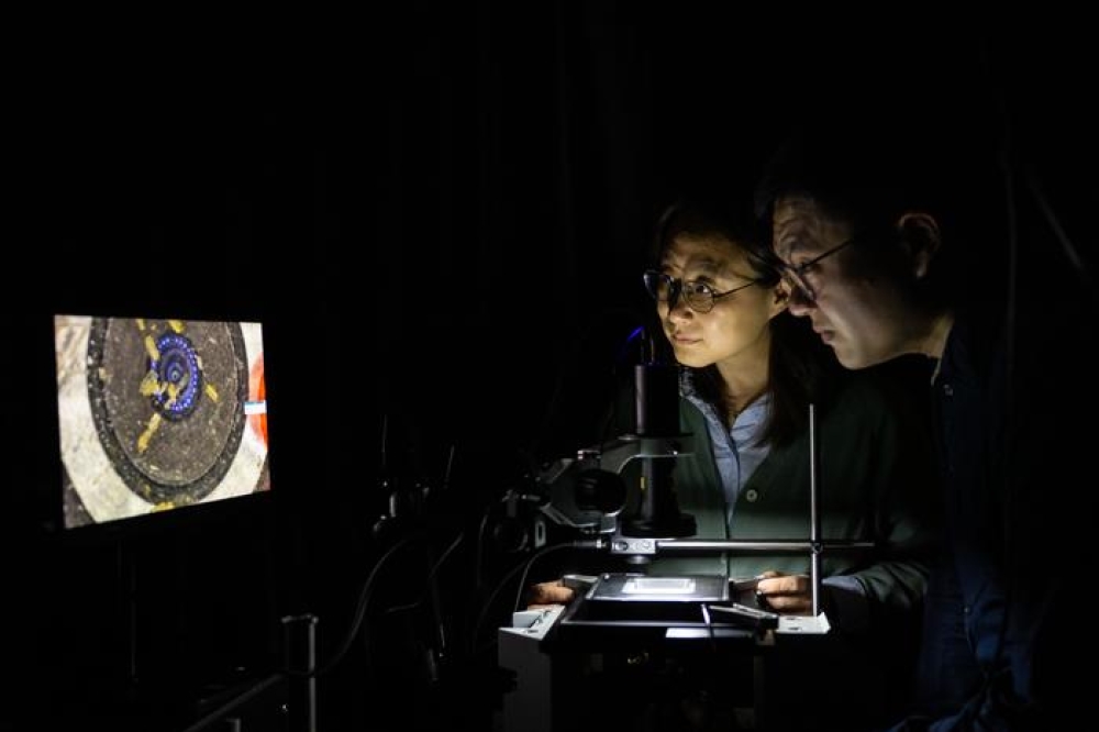
The multi-wavelength laser-based transient thermoreflectance (MWL-TTR) technology enables simultaneous submicron spatial resolution and nanosecond temporal resolution, addressing critical challenges in high-power device thermal management.
GaN HEMTs, while essential for high-frequency and high-power applications, face significant reliability issues due to localised self-heating under extreme operating conditions.
The pursuit of accurate temperature characterisation in GaN HEMTs confronts fundamental limitations of existing methodologies. IR thermography and electrical methods have limited spatial resolution. Micro-Raman thermography approaches normally use below-bandgap probe light sources and would underestimate channel temperatures.
Commercial thermoreflectance reflectance imaging (TTI) techniques commonly use 365nm UV LEDs to characterise the channel temperatures of GaN HEMTs. However, these LEDs affect CCD exposure, resulting in time resolution limited to microseconds. Moreover, UV light induces a photocurrent, whose effect on junction temperature testing has been neglected, according to the researchers.
In addition, they say, there are issues achieving robust thermoreflectance coefficient (Cth) calibration (due to material reflectance inhomogeneity, thermal expansion effects and focus shift), resulting in limited temperature measurement accuracy.
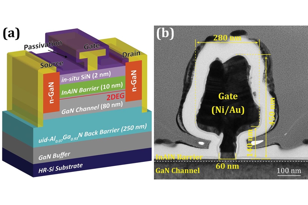
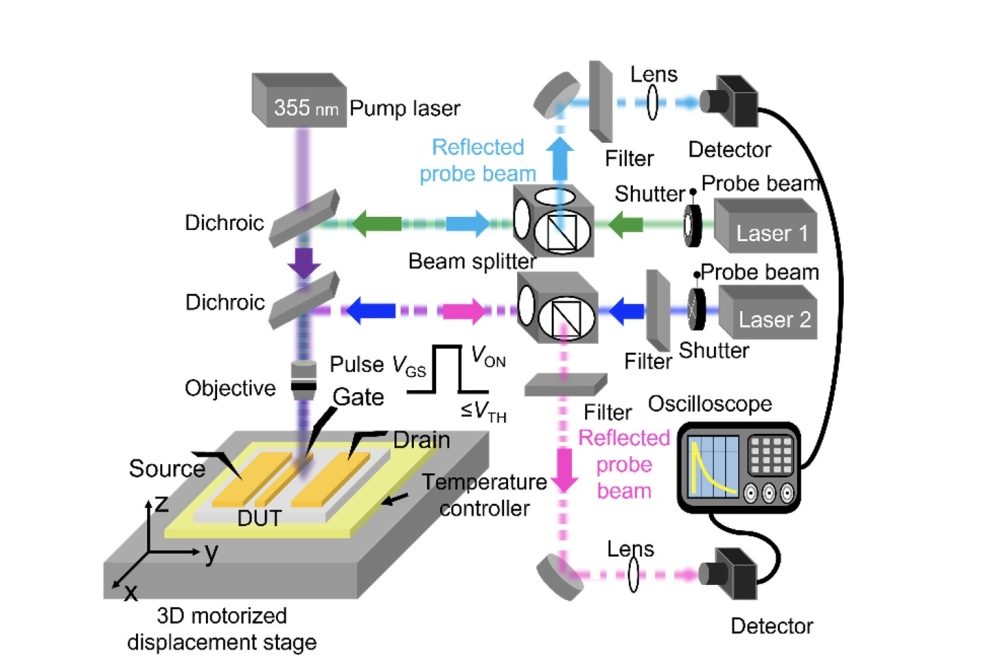
The multi-wavelength laser-based transient thermoreflectance (MWL-TTR) technique uses different wavelengths to measure temperatures in different areas (metal contacts, channels, etc.), as shown in the diagram above.
Compared with the commercial TTI method, using a shorter wavelength (320 nm) to monitor the channel temperature makes the test location closer to the self-heating area on the channel surface, and the test error is better than ±10 percent. The spatial resolution of the test reaches the submicron level, and the temporal resolution in the transient test reaches the nanosecond level.
The 320 nm laser-induced photocurrent has been quantitatively investigated to reduce the photocurrent interference to <5 percent. In addition, the pump-probe transient thermoreflectance method (previously published work: J. Appl. Phys., 134, 115102, 2023; Materials Today Physics, 42, 101367,2024.) has been used for Cth calibration to provide stable and reliable Cth for accurate temperature characterisation.
This new technology successfully maps thermal gradients across critical device pathways. Gate-length directional scans reveal temperature differences exceeding 24 K (>40 percent variation) between gate and drain regions, while gate-width profiles demonstrate 10 K higher channel temperatures compared to adjacent metal contacts. Transient measurements capture thermal dynamics across 50 μs, 100 μs, and 200 μs switching cycles with nanosecond-scale resolution, essential for analyzing GaN devices operating at MHz-GHz frequencies.
In summary, the team says the MWL-TTR technique enables temperature scanning imaging of GaN HEMTs in both transient and steady states, and can also measure other devices like GaAs, Si, SiC, and Ga2O3-based devices. This innovative measurement technology provides critical thermal characterisation capabilities for microwave radio frequency systems and power electronics, where precise thermal monitoring directly impacts device reliability and circuit design optimization.
Furthermore, its compatibility with wide-bandgap semiconductors and dynamic thermal analysis capacity will contribute to manufacturing process improvements, failure mechanism studies, and thermal-aware designs for next-generation electronic devices.
References
Yali Mao, Chao Yuan et al., IEEE Transactions on Power Electronics, Vol. 40, No. 6, pp. 8648–8657 (2025)

