Platinum: A promising contact for p-type SiC
Engineers at Kyoto University have unveiled a promising process for producing low resistivity p-type contacts for SiC power devices.
Forming a low-resistivity ohmic contact on p-type SiC is far from easy – it requires an electrode metal with a work function larger than that of p-type SiC. As that condition is rarely met, when electrode metals are deposited on p-type SiC, this tends to create a high Schottky barrier with a high contact resistivity.
The standard approach for realising a low resistivity is the annealing of Ti/Al-based contacts at 1000 °C. However, the low resistivity that results – it’s in the range 10-6 W cm2 to 10-4 W cm2 – is accompanied by a number of downsides, including electrode melting, surface roughening and device degradation.
Offering an attractive alternative, the team from Kyoto is advocating platinum contacts and an annealing process at just 600 °C. Evidence for the merits of this approach comes from their recent study, involving the evaluation of the characteristics of platinum contacts formed on both circular transmission line model structures and vertical Schottky barrier diodes.
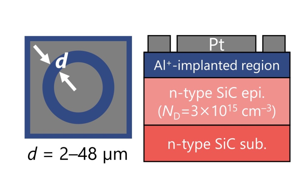
Production of the circular transmission line model structures began with epitaxial growth of 10 mm-thick nitrogen-doped n-type SiC layers on n-type 4H-SiC (0001) substrates. Implantation of aluminium ions into these epitaxial layers at 500 °C created box-shaped profiles with a depth of about 200 nm.
According to secondary ion mass spectrometry, after post-implantation annealing at 1750 °C for 20 minutes under argon, the aluminium doping densities were 8.2 x 1019 cm-3, 1.8 x 1020 cm-3, 2.2 x 1020 cm-3, and 3.0 x 1020 cm-3, depending on the implant dose. Corresponding aluminium atom densities, based on capacitance-voltage measurements of Schottky carrier diodes and estimated Hall-effect measurements, were 3.4 x 1019 cm-3, 5.8 x 1019 cm-3, 6.2 x 1019 cm-3 and 8.3 x 1019 cm-3.
The engineers turned to oxidation at 1300 °C for 120 minutes to remove the surface region of SiC, due to its lack of uniformity in aluminium atom density, prior to cleaning the sample and adding 150 nm-thick platinum electrodes by sputtering. Annealing at either 400 °C, 600 °C or 800 °C created a portfolio of samples.
Formation of Schottky carrier diodes began with the growth of a p-type SiC layers on p-type 4H-SiC (0001) substrates. The addition of platinum electrodes involved the steps employed for the circular transmission line model structures.
Surface profiles, obtained with a white-light interferometer, revealed a root-mean-square roughness of 1.41 nm and 7.04 nm for the platinum electrodes annealed at 600 °C and 800 °C, respectively. This led the team to conclude that annealing at 600 °C significantly suppresses surface roughening of platinum electrodes to far lower values than those for Ti/Al-based contacts annealed at 1000 °C – they have a typical roughness of between 10 nm and 40 nm.
Current-voltage plots were obtained for a range of circular transmission line model structures with an aluminium atom density of 8.3 x 1019 cm-3. These measurements, on structures with various annealing temperatures, as well as no annealing, determined that the platinum contact annealed at 600 °C produced the largest current and an ohmic current-voltage curve.
The team also measured contact resistivity under various annealing temperatures, as well as no annealing, using circular transmission line model structures with an aluminium atom density of 8.3 x 1019 cm-3. As expected, contact resistivity depends on annealing temperature, with the lowest value occurring for annealing of the platinum contacts at 600 °C. Under this condition resistivity is just 3.2 x 10⁻⁵ W cm2, a value that’s said to be as low as that for Ti/Al-based contacts annealed at 1000 °C.
Subsequent capacitance-voltage measurements on Schottky barrier diodes revealed that a higher contact resistivity is associated with an increase in barrier height. Based on this insight, the researchers analysed their contacts with X-ray diffraction, observing peaks from platinum silicides. While the silicon atoms in SiC react with platinum atoms during annealing, that’s not the case for carbon atoms, which are thought to remain near the Pt/SiC interface.
X-ray photoelectron spectroscopy determined the composition of the SiC-metal contact at various depths.
Drawing on all their work, as well as other studies, the team concluded that the platinum silicides are not behind the lower resistivity. Instead, it’s suggested that sp2 carbon, present in an amorphous state, creates several levels in the lower half of the bandgap of p-type SiC that trap holes and shift the Fermi level towards the valence band maxima – and this holds the key to low resistivity.
Pictured above: (a) Schematic illustration of a fabricated Pt CTLM structure
Reference
K. Kuwahara et al. Appl. Phys. Express 18 101003 (2025)