
Fraunhofer IPMS develops wafer-level chiplet systems
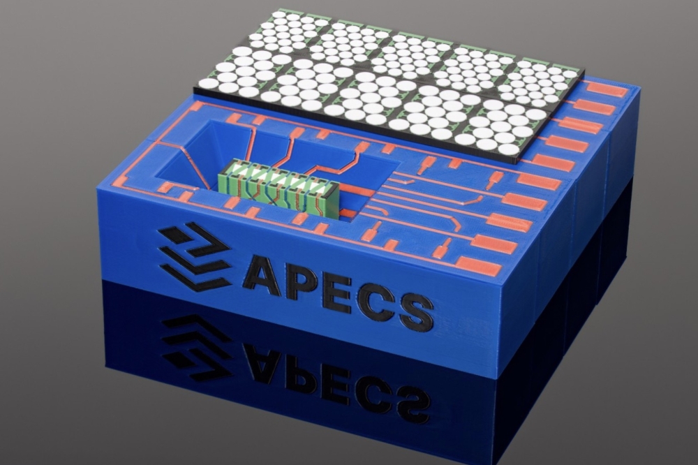
Researchers at Fraunhofer Institute for Photonic Microsystems IPMS have developed a method that allows different chip components to be fused almost seamlessly into a single unit. Their work is part of the European APECS (Advanced Packaging and Heterogeneous Integration for Electronic Components and Systems) pilot line.
By precisely embedding small chiplets into specially structured silicon pockets, Fraunhofer IPMS succeeded in combining the advantages of a compact single chip with the flexibility of modular systems for the first time. This achievement demonstrates the feasibility of quasi-monolithic integration (QMI) and bridges the gap between traditional chip packaging and cutting-edge semiconductor manufacturing.
The aim is to integrate various chip components, such as control electronics, sensors and MEMS, at the wafer level, while retaining the benefits of a compact single chip.
"The basis of QMI is silicon wafers with structured recesses, or pockets. For the first time, dummy chiplets have been inserted into these pocket wafers and the surface has been levelled with a passivation layer in preparation for subsequent back-end-of-line wiring," explains Lukas Lorenz, group leader at Fraunhofer IPMS. "This creates a nearly monolithic system architecture that combines the highest integration density with modular scalability."
QMI technology is said to offer significant advantages over conventional packaging processes. This is due to the way chiplets are arranged on an active or passive wafer substrate with a shared interconnect stack. Since the interconnects are formed in the front-end-of-line process, much higher connection densities can be achieved than with traditional methods.
Lukas Lorenz says: "Although the current demonstrator is based on dummy structures, the process chain can be transferred to real-world customer applications. This enables a scalable integration architecture for future heterogeneous system solutions." Fraunhofer IPMS is targeting industrial partners whose products could benefit from the integration of different high-density technologies. The approaches developed within the APECS framework form the basis for quickly transferring QMI to production-oriented manufacturing environments.
APECS receives funding from the Chips Joint Undertaking and from national grants in Belgium, Germany, Finland, France, Greece, Austria, Portugal, and Spain, as part of the Chips for Europe initiative. The total funding for the APECS pilot line is €730 million over four and a half years.


