Ncodin’s nanolasers eye AI infrastructure
Delivering a revolutionary energy-per-bit, the French start-up’s nanolasers are a compelling source for on-chip communication in tomorrow’s data centres.
BY RICHARD STEVENSON, EDITOR, CS MAGAZINE
Supporting increasing adoption of AI is the building of more and more data centres. This roll-out of essential power-hungry infrastructure already accounts for hundreds of billions of dollars per annum, and total costs are forecast to exceed a trillion dollars a year by the middle of the next decade.
These eye-watering sums offer a fantastic opportunity for companies with technologies that can enhance critical hardware, especially if these products deliver breakthroughs in performance and efficiency.
One of the biggest issues in today’s data centres surrounds the transfer of data between chips. Although widely deployed for decades, copper is a bottleneck to higher speeds. And that’s not its only downside, with other significant weaknesses including a limited reach and losses that lead to a significant contribution to overall energy consumption.
Offering attractive alternatives that address all these issues are various forms of optical links. There are a number of options for the light source – including edge-emitting lasers, VCSELs and microLEDs – and photons can be routed through optical fibres or waveguides in wafers.
Amongst these competing solutions, the French start-up Ncodin, which has just raised €16 million, believes it has the winning formulation: miniature lasers that launch their emission into waveguides in silicon-based wafers. Optical interposers formed by this approach, featuring incredibly small lasers and photodetectors – both are created by the bonding of InP epiwafers to silicon substrates and subsequent photolithography – are claimed to deliver unrivalled efficiencies. Data transfer is incredibly fugal, at less than 0.1 pJ/bit, and integration can exceed 10,000 mm-2, enabling breakthroughs in performance on two fronts – what is possible per Watt, and per dollar.

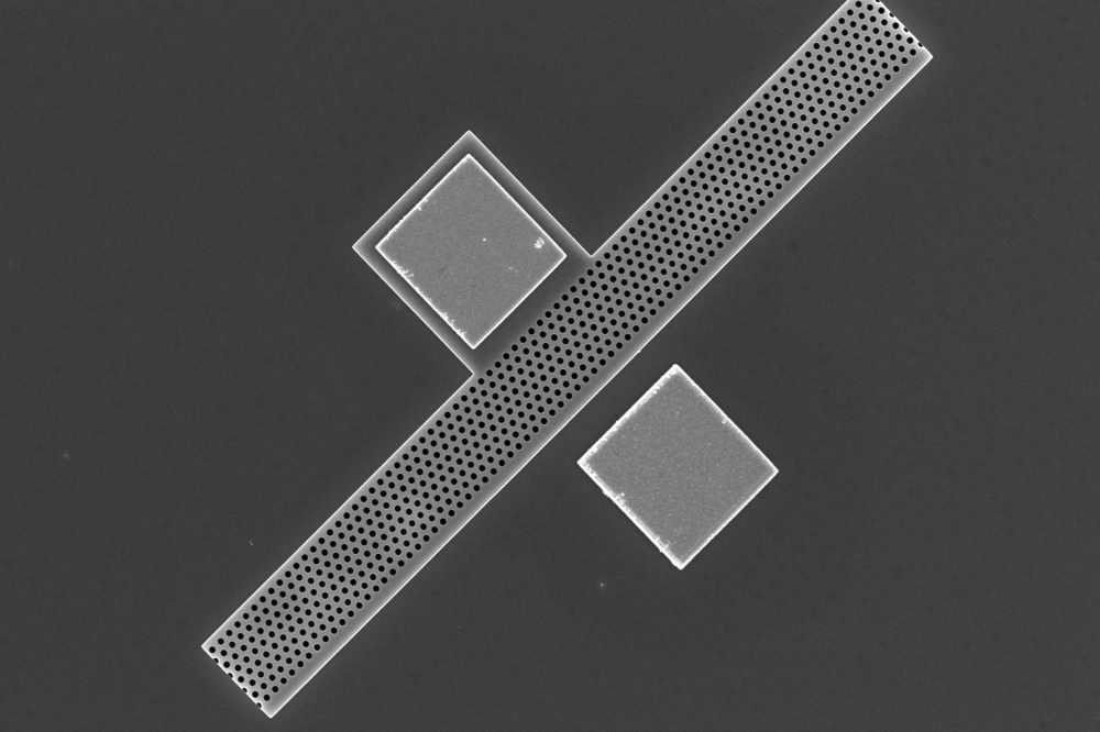
Ncodin’s silicon photonic chip integrating nanolasers, the core technology showing record energy efficiency below 0.1pJ/bit. The wires provide a connection between the controller (an FPGA) and the nanolasers.
A pioneering PhD
The origins of Ncodin can be traced back to the labs at the Centre for Nanosciences and Nanotechnologies, located in the southern suburbs of Paris, where co-founding CEO, Francesco Manegatti, developed these nanolasers during his PhD days.
Enthused by the emergence of a start-up ecosystem – in 2017, colleagues from this lab founded the quantum computing spin-off Quandela – Manegatti shifted his post-graduation plans from joining a big company to trying to commercialise the nanolaser technology he’d developed, a vision shared by his supervisor, now chief scientific officer and co-founder Fabrice Raineri.
Efforts in this direction began in late 2019 and continued during the pandemic, when these entrepreneurial partners started to try and secure initial funding and develop a first roadmap towards commercialisation.
The next steps involved: working with the support of CNRS on an R&D project; establishing a business plan; and bringing in the third co-founder, Bruno Garbin, who switched roles from a postdoc in the laboratory to Ncodin’s CTO.
Founding of the start-up followed in 2023, with Ncodin raising €3.5 million in a pre-seed funding round that closed in March 2024. Since then, headcount has mushroomed from four to 30 employees, and the company has established its own headquarters.
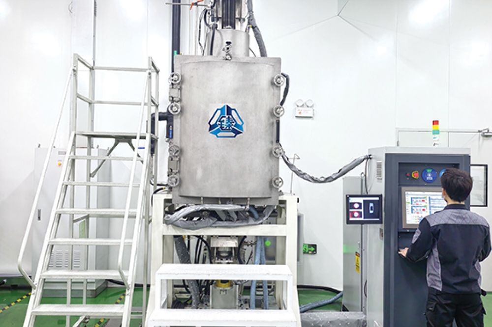
“We still exploit the facilities of CNRS, because this lab has the largest academic clean room of France. It's a 3,000-squared-metre clean room, where they have a lot of collaboration with private entities,” explained Manegatti
Ncodin uses this facility to develop its chip technology, and make proof-of concept devices that are shared with partners.
“In parallel, we are working on the industrialisation of our technology, to reproduce it in a CMOS pilot line on 300 millimetre [wafers].”
The start-up has always focused on optical interconnects, Neuromorphic architectures initially garnered consideration, but the primary goal is to complement copper and aid the scaling of infrastructure and process architecture.
“For extremely short reach, copper is best,” argues Manegatti. “It's super resilient, it's super robust, you can deliver a high bandwidth.”
But for connections beyond a few centimetres, links should switch to the optical domain, where Ncodin’s solution addresses the challenge of transferring tens of terabits per second of bandwidth while consuming just a fraction of a picojoule per bit.
This is an attractive option for AI workloads, which are fulfilled through continuous communication between the compute element, which could be a GPU or an ASIC, and the high-bandwidth memory. For these tasks, nano-lasers promise to play a role in fulfilling demands for extremely fast retrieval of data, as well as the writing of data in the memory.

Since its founding in 2023, headcount at Ncodin has increased to 30 employees.
Numerous nano-laser
To produce its devices, the French start-up draws on external expertise for the growth of its epiwafers. Multiple coupons are crafted in these epiwafers, prior to hybrid bonding to silicon-based wafers. Subsequent lithography and patterning define the dimensions of lasers and photodetectors, both operating at telecom wavelengths. The emission from the lasers, which have a footprint that is 500 times smaller than their conventional cousins, evanescently couples into the waveguides in the underlying silicon wafers.
Nanolasers produced by this process have an output of up to a few hundred microwatts – that’s more than enough for the intended task – and an efficiency of around 15 percent. These low emitting powers prevent self-heating issues for the miniature sources, which are capable of delivering robust operation at temperatures approaching 100 °C.
Thanks to the incredibly high density that can be realised with Ncodin’s technology, the intention is to connect every input and output pin of every ASIC and every high-bandwidth memory to a nanolaser.
“Our goal is, of course, to add redundancy, to extend even further the lifetime and essentially the reliability of our chip,” adds Manegatti.
The nanolasers are directly modulated, as it’s not critical to have a high data rate per channel, thanks to the use of so many channels.
According to modelling by Ncodin, it’s possible to realise data rates of up to 64 Gbit/s. However, the nanolasers currently operate at 16 Gbit/s.
“This is more than enough,” argues Manegatti. “High-bandwidth memory, for example, is driven at 8 gigabits-per-second today.”
Before Ncodin’s optical interposers are deployed in data centres, they need to have proven reliability. Efforts in this direction are on-going, according to Manegatti, who remarks: “We are industrialising the solution, so the most important KPIs will be extracted during this project.” Note, though, that his team have already demonstrated lifetimes that are well beyond a few thousand hours.
The business plan
To produce its technology in volume, Ncodin will partner with a dedicated foundry to manufacture wafers packed with optical interposers.
“We'll sell the wafers to our customers, so chipmakers like Nvidia, Qualcomm, AMD, Intel, et cetera,” says Manegatti. These household names will employ partners to test, assemble and package entire systems that combine Ncodin’s wafers with a variety of chips, such as those for memory and processing.
Manegatti says that the main goal for now is to finish the industrialisation project, undertaken with a partner, and start qualification of its product.
“We're going to open an office in Silicon Valley, to be closer to our customers and partners, and to be able to engage in an even deeper relationship with them.”
These plans, which make a lot of sense, promise to enable III-Vs to play yet another role in tomorrow’s technology infrastructure.