Fraunhofer IPMS expands ultratrace elemental analysis
The Fraunhofer Institute for Photonic Microsystems IPMS is expanding its analytical capabilities in the field of wafer contamination.
In a dedicated laboratory, the established method of vapour phase decomposition is used in combination with inductively coupled plasma mass spectrometry (VPD-ICP-MS). This combination enables precise monitoring of wafer surface contamination, according to the Institute.
Various characterisation methods are used to detect and quantify wafer contamination. Fraunhofer IPMS has expanded these methods to include ultratrace element analysis. After etching 200- or 300-millimetre wafers with hydrofluoric acid vapour, a droplet is applied to the wafer surface and moved across it.
The droplet collects the soluble residues present on the surface and is then diluted to a volume of 1 ml. The dissolved elements are then analysed using inductively coupled plasma mass spectrometry (ICP-MS). This process provides accurate quantitative information about the soluble elements on the wafer surface.
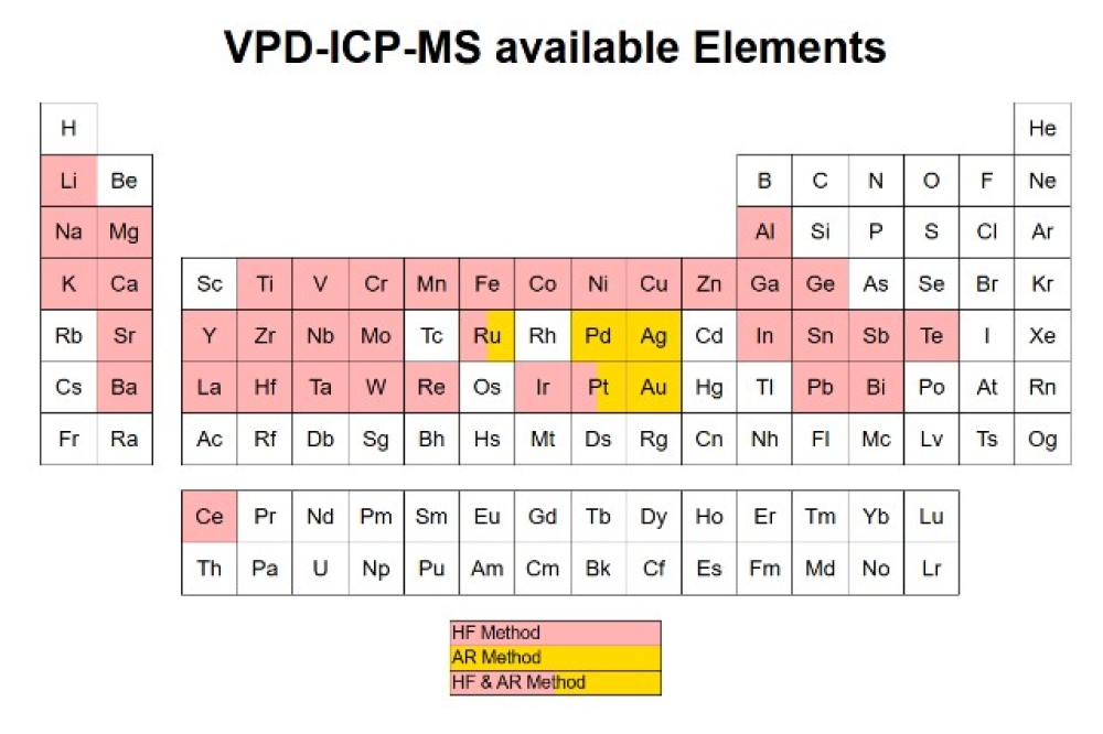
Ultratrace element analysis provides a wide range of possibilities. Surface and bevel scans are performed using an HF scan solution to analyze 39 elements, enabling detailed characterisation of the wafer surface. For specific applications, aqua regia can be used as a scan solution for five noble metals.
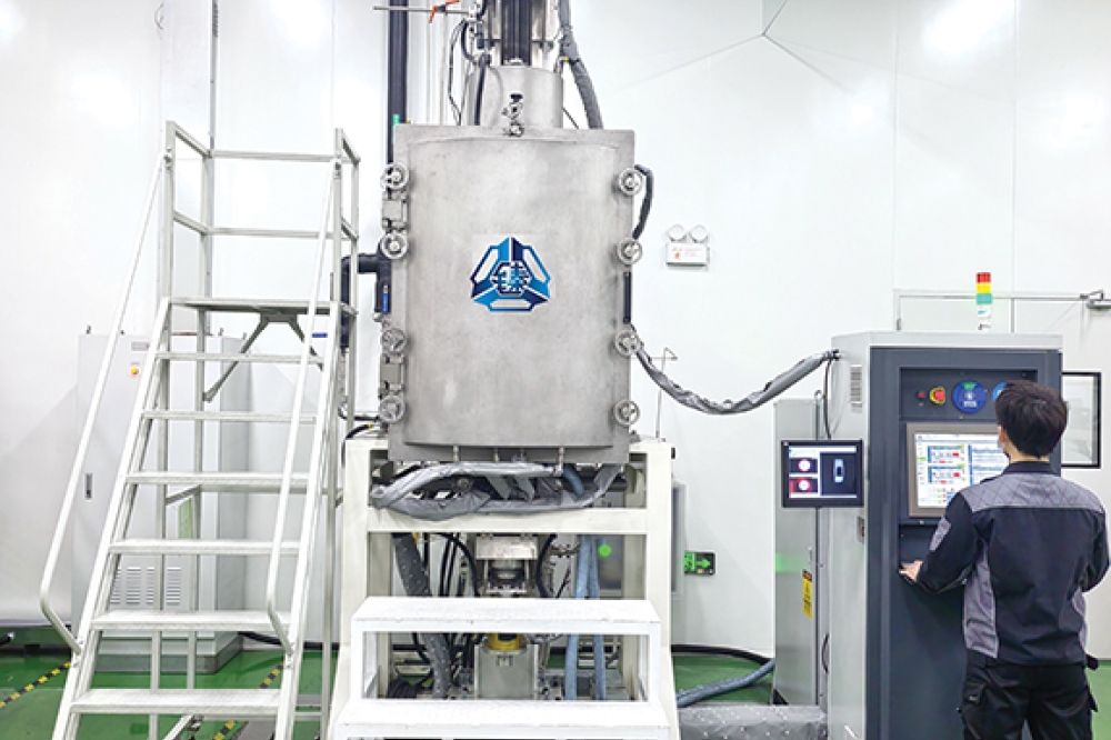
The laboratory is equipped with the WSPS2 Wafer Surface Preparation System from PVA Tepla and the iCap RQ mass spectrometer from Thermo Scientific. These technologies enable accurate characterisation and quality assurance in the semiconductor industry.