
The pros and cons of PCSELs and VCSELs
While the VCSELs is a proven technology that’s serving in two killer applications, it has weaknesses that are addressed by the PCSEL, a promising technology on the cusp of commercialisation.
BY RICHARD STEVENSON, EDITOR, CS MAGAZINE
Edge-emitting lasers are an unquestionable success. Over a number of years, they have been deployed in a wide variety of applications, including optical networks and cutting and welding, and will have generated sales worth billions and billions of dollars. But they have significant weaknesses: modulation rates are not that high; testing and packaging is far from easy; they are expensive to produce; volumes are mediocre; and the emission profile is not the desired circular beam.
Addressing all these issues are surface-emitting lasers. The most well-known and mature of these is the VCSEL, which has been manufactured in volume for many years, and has found deployment in two ‘killer’ applications: short-reach optical links, and a light source for facial recognition in smartphones.
A key limitation of the VCSEL is its spectral range. High-volume products emit in the infra-red, typically at 850 nm or 980 nm, with optical gain supported by a pair of mirrors, each made from alternating layers of GaAs and AlGaAs. Expanding the spectral range involves the production of mirrors emitting in the visible or further into the infra-red, but it’s challenging to find material pairings that combine conductivity with a sufficient refractive-index contrast and lattice constants close enough to ensure high-quality epilayers.

Figure 1. Wavelength at a 5 mA drive current (top row) and
threshold current density (bottom row) for GaAs VCSELs grown on 150 mm
germanium substrates with different thicknesses. All VCSELs have a mesa
diameter of about 49 mm and an oxide aperture of about 14 mm. For more details
see S J Gillgrass et al. J. Phys.
Photonics 7 035033 (2025).
The PCSEL – short for photonic-crystal, surface-emitting
laser – avoids this issue, with optical gain realised by in-plane feedback.
Thanks to this design, the PCSEL provides emission over a far wider spectral
range.
What’s not clear is when the PCSEL will start to fulfil its promise and generate significant sales. Many applications could be served, but where is this class of laser going to make a commercial impact? Meanwhile, progress in VCSELs continues, pushing performance, with new processes that minimise strain and help to expand the spectral range.
Insights into all these matters and more were provided by speakers at this year’s CS International, held on 21-22 April at Sheraton Brussels Airport Hotel. At this upbeat gathering of leaders in industry and academia, presentations detailed: the merits of switching from GaAs to germanium substrates for the production of GaAs-based VCSELs; how etching offers an attractive to solution to producing mirrors for InP VCSELs; demonstrations of the PCSEL for light-based, high-speed communication; and where the opportunities may lie for PCSELs to excel.

Yale academic and Chief Scientist at InPhred, Jung Han, has
developed an electrochemical etching technology that enables the production of
lattice-matched InP DBRs.
Switching foundations
While GaAs provides an effective foundation for the
production of the GaAs-based VCSEL, it’s not perfect. There is a small but
significant lattice mismatch between GaAs and AlGaAs, and when the resulting
strain is magnified by growing high-reflectivity distributed Bragg reflectors
(DBRs) with many tens of layers, epiwafers are no longer flat. Offering an
attractive alternative is the germanium substrate, which has a lattice constant
sitting between that of GaAs and AlAs.
This approach has been pioneered by IQE and its collaborators. Work continues, with an update provided at CS International by the Managing Director of the Institute of Compound Semiconductors, Peter Smowton.
He told delegates that today’s standard manufacturing platform for the VCSEL, which is in great demand for 3D sensing and communications, is the 150 mm GaAs substrate.
“We expect it to move to 200 mm, and in fact VCSEL material has been available on 200 mm substrates since 2022,” said Smowton, who added that IQE is behind this breakthrough.
He pointed out that concerns associated with the GaAs substrate are not limited to epiwafer bow. “Gallium arsenide is not recycled to any large extent, and it’s difficult to recycle, so that’s an environmental issue. And 90 percent of gallium comes from a single country [China], with the other 10 percent coming from Russia, so that is somewhat problematic.”

Figure 2. InPhred is pioneering the use of electro-chemical
etching to produce InP-based VCSELs.
In comparison, while 60 percent of germanium comes from
China, there are many sources, and it’s possible to recycle the material. In
addition, as well reducing wafer bow, germanium substrates are more robust,
opening up the possibility to use thinner substrates and reduce wafer breakage;
and substrates are available in sizes up to 300 mm, offering a pathway to
greater economies of scale.
However, despite all these merits, VCSEL manufacturers are reluctant to switch to germanium, which is more expensive – for the 200 mm format, prices are twice as high as those for GaAs.
Device manufacturers will not certainly not make the switch if it leads to a significant reduction in the performance of the VCSEL. And to see whether that is the case, Smowton and his colleagues have been evaluating the performance of a what is referred to as a fairly generic 940-nm-emitting structure, featuring a single oxidation layer for current confinement. VCSELs have been produced on GaAs and germanium substrates with 150 mm and 200 mm diameters.
When this VCSEL structure is grown on 150 mm GaAs, there’s between 130 µm and 150 µm of wafer bow, while for the 200 mm format bow is above 200 µm. For germanium, there’s warping, but the distortion is much diminished.
What’s described as ‘fast-fab’ structures have been produced at the Institute of Compound Semiconductors, with 150,000 devices on 150 mm wafers, and 280,000 on the 200 mm format.
Comparisons of VCSELs on 150 mm substrates show that germanium provides a superior thermal impedance. When considering other metrics, these two types of emitter produce characteristics that Smowton refers to as “pretty much identical”.

Figure 3. The InPhred process for producing VCSELs.
Given the relatively high price of germanium substrates
compared with GaAs, Smowton and colleagues have investigated VCSEL performance
on thinner foundations that could trim costs – they are two-thirds and
one-third as thick. For this work, VCSELs were optimised for the thinnest
substrate.
Maps of emission wavelength and threshold current density are similar for VCSELs produced on substrates with thicknesses of 675 µm and 450 µm (see Figure 1). There’s a greater spread for lasers on 225 µm-thick substrates, with a region with leaky devices, due to warp that hampers processing in a conduction furnace. “If it was in a convection furnace, that wouldn’t be an issue,” remarked Smowton.
For investigations with 200 mm material, the team employed a VCSEL production process that’s optimised for the GaAs substrate. Growth of germanium produced VCSELs with a slightly wider distribution in emission wavelength and threshold current density. When considering a threshold current of no more than 5 mA, yield on GaAs is 97 percent, while that on germanium 93 percent.
Commenting on this result, Smowton said that there’s still work to do, including the need to optimise epitaxial growth for 200 mm germanium.
InP VCSELs
VCSELs emitting at wavelengths beyond 1.1 µm are attractive
candidates for next-generation sensing, digital health, and data centre optical
interconnects. But to reach this spectral domain, device designers have to move
away from the conventional material system, based on GaAs.
For many years, effort has been directed at this issue. Progress has included VCSELs by Corning and Vertilas, featuring epitaxial DBRs that are lattice-matched to InP; VCSELs with strained active regions, such as the dilute nitrides used by Hitachi, and the InAs quantum dots pioneered by the Technical University of Berlin; and variants with an air-gap DBR on an InP substrate, a design pursued by Agilent. More recently, Vertilas has turned to double dielectric mirrors, and a number of other teams have pursued wafer fusion with AlGaAs DBRs.
Pioneering yet another approach, based on lattice-matched InP, is Yale University spin-off InPhred.
Speaking on its behalf at this year’s CS International, company Chief Scientist Jung Han, who is also an academic at Yale, explained that the core technology can be traced back to work undertaken about 15 years ago, involving electrochemical etching.
According to Han, when n-type GaN is placed in a solution and a negative bias applied to the electrolyte, electrons are injected from the valence band to the conduction band. This creates holes on the surface, which weaken the semiconductor, leading to oxidation and etching.
“When everything is done right, you can create very, very tiny air bubbles or voids in otherwise single-crystalline perfect semiconductor,” added Han. “Once you introduce these tiny nanoscale bubbles, the index of the semiconductor drops very, very quickly.”

Vector Photonics, led by its CEO and co-founder Richard
Taylor, has demonstrated that PCSELs can provide free-space transmission over
hundreds of metres. Using a system designed and built by Fraunhofer UK, data
transfer has been realised at 50 Mbit s-1 at a distance of
500 m. This is a real-world result, with transmission over the river
Clyde, from the Glasgow Science Centre to the Clydeside Distillery.
As the etching depends on the conductivity of the material,
if the electrochemical process is applied to an InP stack with alternating
layers that are heavily doped and undoped, the resulting structure will feature
alternating low-refractive index, nano-porous layers, and
high-refractive-index, pristine layers (see Figure 2).
“If the thickness is right, it will give you a DBR stopband with pretty much 99.9 percent reflectivity, and you can tune the stopband,” enthused Han.
In addition to lattice-matching, mirrors benefit from relatively few alternating layers. Thanks to a refractive index contrast of up to 1.0, a reflectivity of around 99.5 percent is realised with 10 or so mirror pairs.
Han explained that the VCSEL fabrication process begins with homoepitaxial growth of the structure, which includes a tunnel junction. Engineers then form a mesa, define an aperture with ion implantation, and form an optical aperture. A side wall is then exposed, allowing electrochemical etching, prior to passivation, metallisation, and the addition of a p-type DBR (all these steps are illustrated in Figure 3).
Using this approach, engineers at InPhred have produced VCSELs with emission wavelengths from 1300 nm to 1700 nm using nearly identical processes. Peak power conversion exceeds 29 percent; the threshold current density for emitters with a 10 µm-diameter aperture is 1.0-1.4 kA cm-2; and VCSELs have passed the Telecordia 468 reliability test, involving operation for 2,000 hrs at 85 °C.
Han also presented preliminary results for linear VCSEL arrays with a handful of apertures. Encouragingly, output power is proportional to the number of apertures.
According to the Chief Scientist, the leading application for the company’s InP VCSELs is 3D sensing, time-of-flight measurements. For sources beyond 1400 nm, emission is in the eye-safe regime, and the detection background quieter.
The other application that the start-up is targeting is optical interconnects, where it will compete with the likes of silicon photonics.
According to Han, InP VCSELs are strong contenders in this sector, by combining telecom-wavelength compatibility with the wafer-scale manufacturability and packaging simplicity of VCSELs. When serving in AI hardware, they promise to provide energy-efficient single-mode optical links, outperforming GaAs VCSELs and silicon photonics.
PCSELs for Li-fi…
Another speaker at this year’s CS International, Vector
Photonics CEO Richard Taylor, championed the merits of the PCSEL, arguing that
they deliver the performance of an edge-emitter in a surface-emitting form
factor. This is said to deliver several key advantages, including: wavelength
flexibility; high beam quality; design of line width; and the opportunity to
make large-scale, coherent arrays.
Taylor explained that Vector has a distinctive approach to producing PCSELs. “The traditional way is a void-containing structure, where you etch a grating, you do epitaxial regrowth, and you encapsulate air structures within the photonic crystal,” remarked the Vector CEO. “What we do is very similar, except we infill the holes and have an all-semiconductor platform.”
According to Taylor, removing air-filled structures from the device increases reproducibility, manufacturability, and reliability. These gains are realised, because when voids are present, they increase variability in device characteristics.
Vector has produced PCSELs with various material systems, but at CS International, Taylor only discussed breakthroughs associated with emitters made from InP. “We’ve got devices packaged in TO cans, we can do WDM [wavelength-division multiplexing], and we’ve got relatively good optical output powers compared to DFBs,” said Taylor, adding that devices have been demonstrated in real-world systems.
Recently, effort has been directed at investigating the reliability of the lasers. “We previously demonstrated 2,500 hours, and more recently increased the acceleration factor to over 100 at 1,500 hours.” The reason for cranking up this factor is to understand the failure mechanisms for these PCSELs. Taylor added: “If anyone knows about forcing failure modes in lasers that can help us out, please let us know, because it turns out they are very resilient.”
As well as a high level of reliability, Vector’s PCSELs provide excellent control of the emitted wavelength, thanks to the opportunity to tune the grating. Sub-nanometre precision is possible, alongside exceptional reproducibility, highlighted by results from a 3-inch InP wafer that provided several thousand PCSELs. “We randomly selected 60 of them across different device sizes,” remarked Taylor, who added that they found a variation in emission wavelengths of just ± 0.1 nm.
One promising application for the PCSEL is laser-based free-space optical communication in challenging environments, such as war zones and disaster areas. To demonstrate the capabilities of this technology, Vector is partnering with Fraunhofer UK, to build free-space optical communication systems.
According to Taylor, PCSELs are ideal for this task, with a large emitting area enabling a high output power, and a low-divergence aiding detection of the signal.
The first system, held back by drive electronics, transmitted data over 200 m at 50 Mbit s-1. Since then, speeds have increased to 700 Mbit s-1, and very soon the partnership is expecting to exceed a gigabit-per-second, over 1 km.
Another application where the PCSEL has much potential is secure communication. Recently, Vector demonstrated how PCSELs can transmit orbital angular momentum, a first step in a quantum key distribution system.
According to Taylor, the traditional approach to producing a source of orbital angular momentum is to direct the emission from a laser through an external Q-plate – but this requires a large, bulky system.
Working with the UK’s Compound Semiconductor Applications Catapult, Vector reduced the size of a source of orbital angular momentum, initially with a fibre-based system, and more recently, by 3D printing a waveplate. Initially printed on glass, waveplates are now directly printed on the device.
… and other applications?
Another pioneer of the PCSEL is Huawei’s Bragg Research Centre, which is based in Ipswich, UK.
Speaking on behalf of this facility, CTO Graham Berry explained that it develops and manufacturers edge emitters and surface emitters. “We’re relatively agnostic, and what we tend to do is choose the technology based on the performance and the packaging optics.”
Berry focused on the choice of source for interconnects for AI-orientated data centres, saying that the two leading approaches are to either have high data rates at a single wavelength, or employ multiplexing and a range of wavelengths. “At the end of the day, the overall power consumption will be the prevailing winner,” argued Berry.
He pointed out that PCSELs offer a low-cost packaging route, with options for data transfer including multi-fibre push-on connectors, and fibre arrays. For these technologies, the 850 nm VCSEL is not ideal, as it is not suited to single-mode fibre – to do so demands a very small aperture – and emission is beyond the cut-off window.
For the PCSEL, the diameter of the emitter can be as small as a few microns, and potentially up to 10 mm. For all these sizes, it’s single mode. “So, you have a platform for high power, mid power, and potentially some form of slow and fast,” remarked Berry, who pointed out that another merit of the PCSEL is that it tends to avoid catastrophic optimal damage, thanks to power scaling with the area of the emitter.
In addition, PCSELs provide a very high beam quality and narrow beam divergence. “If you want to go lens-free and develop really small form factor micro-optics, being able to take the lenses out of that system is quite a nice win,” argued Berry.
One downside of the PCSEL is its threshold current density, which tends to be higher than an edge emitter, due to scaling with area. “When you’re after the last ounce of wall-plug efficiency, this threshold can come back to hurt you a little,” warned Berry, who pointed out that it’s not possible to produce PCSELs with apertures as small as VCSELs, because optical leakage kicks in at diameters below 20 µm.
With PCSELs, due to the limited number of devices produced so far, it’s difficult to gauge reliability. “But there are no red flags at the moment,” said Berry.
Discussing the potential for PCSELs to displace VCSELs in more detail, Berry considered VCSELs with apertures below 3.5 mm that provide single-mode operation, and could target 1 pJ bit-1. He pointed out that while realising a bandwidth of 40 GHz with this design of VCSEL is challenging, it has been realised in the lab. However, small apertures may hamper reliability.
Link length is also a concern. For 850 nm VCSELs, connections are typically limited to 60 m, but there is the potential to extend to 100 m. Moving to 1060 nm VCSELs lengthens the link, with distances of 500 m and 2 km possible using multi-core and single-mode fibre, respectively.
Comparing these strengths and weaknesses with PCSELs, Berry remarked: “Our sweet spot on the PCSEL is between 200 and 400 microns, and it’s as a high-power light source.” Another merit of the PCSEL is that it’s suitable for wavelength-division multiplexing. “The challenges are the slope efficiency.”
PCSELs could also serve as the external light source for silicon photonics, with devices in small pluggable form factors providing between 200 mW and 400 mW.
“400 milliwatts would support something like 8 channels in silicon photonics,” said Berry, who added: “If you could go to 800 milliwatts, you potentially could do all 16 channels.”
For this application, Berry believes that laser efficiency needs to be at least 25 percent, a performance realised at an operating temperature of at least 50 °C. The team at Huawei is not far from those requirements, with PCSELs producing potentially 300 mW over that temperature range, and recent work by Sumitomo showing that this class of laser is capable of output powers of 800 mW.
So PCSELs undoubtedly have much promise, and opportunities in many markets. But whether they’ll ever enjoy sales as large as those of the VCSEL remains to be seen.
In 2027, CS International will be held on 13-14 April at the Sheraton Brussels Airport Hotel.
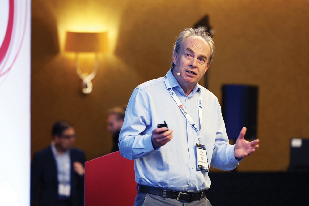
Main image: Peter Smowton, an academic at Cardiff University and the Managing Director of the Institute of Compound Semiconductors, oversees efforts to improve the production of VCSELs by shifting their foundation from GaAs to germanium.


