
SiC: Enhancing reliability with ion implantation
By stopping the movement of partial dislocations, high-energy ion implantation provides an approach for improving the reliability of SiC devices.
BY MASASHI KATO AND TONG LI FROM NAGOYA INSTITUTE OF TECHNOLOGY, SHUNTA HARADA FROM NAGOYA UNIVERSITY, AND HITOSHI SAKANE FROM SHI-ATEX
Over the last few years, SiC power devices have started to fulfil their tremendous potential. Sales are climbing fast, with global revenues now worth several billion dollars per annum, thanks to the deployment of these devices in trains and electric vehicles.
However, there’s still substantial room for improvement in the manufacture and performance of these power devices, which tend to be produced using the 4H-SiC polytype. One issue is a high cost, which hampers penetration in hybrid electric vehicles, electric power sources for data centres, and other applications. This weakness is exacerbated by concerns surrounding manufacturing yields for devices that guarantee long-term reliability.
One phenomenon impairing the long-term reliability of SiC power semiconductor devices is bipolar degradation. This occurs when a current flows through a p-n junction, injecting electron-hole pairs into the material. After penetrating the drift layer, electron-hole pairs recombine in the 4H-SiC substrates at basal plane dislocations (BPDs) – they are dislocations located on the (0001) crystal plane of 4H-SiC. This is not the end of the story, as each BPD splits into two partial dislocations (PDs), which lead to the formation and expansion of stacking faults (SFs) in the epitaxial layer surrounding the PDs.

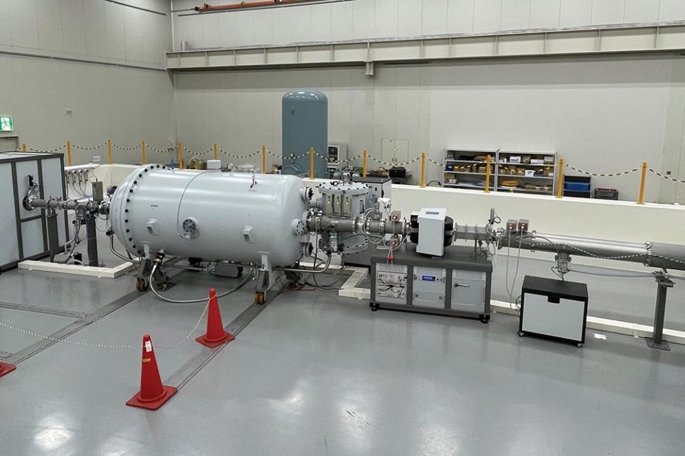
Figure 1.The tandem-type accelerator in Shi-Atex for high-energy ion
implantation of SiC. The accelerator is located at the top of the photo,
while the wafer handling stage is located at the bottom.
These expanded SFs are behind the degradation in performance of SiC power devices. Contributing to the electrical resistance component in the forward diode characteristics, they provide the source for the leakage current.
Complicating matters, degradation is difficult to detect during initial device operation. This is a significant issue, with reduced manufacturing yield accompanied by an increase in the cost of reliability testing.
A number of approaches have been pursued to reduce the injection of electron-hole pairs, and ultimately suppress SF expansion. One method involves the introduction of a recombination-enhancing layer between the drift layer and the 4H-SiC substrates. This addition eliminates the injected electron-hole pairs, so they no longer reach the substrate. Another strategy, explored by several groups, is to use SiC MOSFETs with embedded Schottky barrier diodes. This combination quashes the generation of electron-hole pairs, even at active phases of diode operation. However, none of these technologies delivers a complete solution to bipolar degradation.
Offering an innovative alternative to address this problem is our team, a long-term collaboration between Nagoya Institute of Technology, Nagoya University and Shi-Atex, a company with tremendous expertise in high-energy ion implantation technology.
Our partnership draws on a strong academic background in materials science that spans semiconductors and metals. This led one of us, Shunta Harada, to introduce a new idea for preventing the degradation of SiC power devices via the intentional introduction of impurities, such as hydrogen. Critical to the success of this approach is fixing the impurities to BPDs, a step that stops the movement of PDs that make up BPDs. Once the movement of PDs is halted, expansion into SFs is prevented. Note that this is a similar concept to hardening metals, such as iron becoming steel through the introduction of carbon impurities.
Key to our investigation is the tandem-type accelerator owned by Shi-Atex (see Figure 1). This accelerator has enabled us to apply high-energy ion implantation to SiC power devices, a step that promises to suppress bipolar degradation. Initial progress was assisted by students at Nagoya Institute of Technology, before Tong Li joined the team, supporting widespread utilisation of high-energy ion implantation for SiC power devices.

Figure 2. Schematic of a SiC epitaxial wafer and depths of ion
implantation. With standard ion implantation, ions cannot reach the
interface of the epitaxial layer and the substrate.
Rationale for high-energy ion implantation
During conventional ion implantation into 4H-SiC, ions reach a depth of less than 1 µm, because accelerated energies are usually below 1 MeV. To put that depth into context, note that 4H-SiC epitaxial wafers have epitaxial layer thicknesses between 5 µm and 60 µm, and a typical substrate thickness of around 350 µm.
In our case, as we want to stop the movement of PDs in the substrate near the epitaxial layer, we need the implanted ions to reach the interface of the epitaxial layer and the substrate. To fulfil this objective, we use high-energy ion implantation, shown schematically in Figure 2.
Let’s consider a SiC power device with a typical voltage rating. Based on this criterion, we have selected a 1.2 kV-class device that has an epitaxial layer thickness of 10 µm. To implant hydrogen ions (protons) to the interface from the epitaxial layer surface, we require an acceleration energy of around 1 MeV; and to reach this interface from the substrate side, we need much higher energy of around 8 MeV (in fact, we have only achieved an implantation depth of around 330 µm so far, but even this is effective for our purpose). Note that even higher implantation energies are needed if we employ heavier ions. For example, implantation of helium ions to a 10 µm depth requires around 3.6 MeV.
Reliability testing
We began our investigations into the effect of high-energy ion implantation on SF expansion by using UV illumination and X-ray topography to observe any changes to 4H-SiC epitaxial wafers. Without high-energy ion implantation, and prior to UV light illumination, the BPDs appear as straight lines in the X-ray topography images. But after UV light illumination, the BPDs expand into SFs in the epitaxial layers, appearing as triangles in the X-ray topography images.
With high-energy ion implantation, this situation changes markedly. In this case, the BPDs kept the same straight lines in X-ray topography images after UV illumination. This observation confirms the effectiveness of high-energy ion implantation.

Figure 3. Prober (the top) with power sources and a temperature controller (the bottom) for electrical stress tests for SiC p-i-n diodes.
Following this confirmation, we applied our technique to devices, fabricating p-i-n 4H-SiC epitaxial wafers. Our process involved aluminium-ion implantation into the epitaxial layer to create a p-type layer on the surface. We then performed activation annealing of aluminium, an acceptor impurity, at typically 1650-1750 °C. Using photolithography and subsequent lift-off of the metal, we added metal contacts on the
substrate-side and patterned metal contacts on the surface-side. Finally, we annealed the wafer, forming an ohmic contact by reaction of the metals and 4H-SiC.
We conducted high-energy ion implantation on bare 4H-SiC epitaxial wafers before forming our p-i-n diodes. This approach is adopted because after high-energy ion implantation, high-temperature annealing is required to recover damages caused by implantation. Without this, the p-i-n diodes would have a very high series resistance.
Initially, we implanted protons from the epitaxial side of the bare epitaxial wafers. Using additional wafers, we implanted helium ions from this side to assess the effects of different ions; and implanted protons from the substrate side, to determine the impact of backside implantation.

Figure 4. A diode under probing. The diode is placed at the centre of
the stage, and electrical power applied to the diode from the wire at
the left-hand side. The thin probe is a thermocouple, to detect the
temperature of the diode.
Using electrical stress tests, we investigated the reliability of our implanted and conventional p-i-n diodes, considering their susceptibility to bipolar degradation. Our study involved applying pulsed currents from 200-850 A cm-2, with the particular value depending on diode performance.
These measurements involved a prober system with power sources and a temperature controller (see Figure 3, and Figure 4 for a photo of a p-i-n diode under probing). During measurements, temperature was monitored by the thermocouple and fed back to the temperature controller.
During and before/after the test, we observed SF expansion in electroluminescence images, obtained though stripes of the patterned contacts on the epitaxial layer surfaces. The dark regions observed in the electroluminescence images correspond to locations with expanded SFs.
As expected, our p-i-n diodes that have not benefited from high-energy ion implantation suffer from a significant number of expanded SFs. These faults are seen in the dark regions in the electroluminescence images (see Figure 5, which provides an example of uniform and nonuniform electroluminescence images for before and after stress, respectively).
In stark contrast, our p-i-n diodes that have the advantage of high-energy ion implantation enjoy significantly reduced SF expansion, and their electroluminescence images are relatively uniform, even after stress. This is a repeatable finding – we have obtained reproducible results, demonstrating that p-i-n diodes with high-energy ion implantation show a significantly smaller number of expanded SFs. Note that suppression of SF expansion is effective, irrespective of the type of implanted ions (protons or helium ions) and the implantation side.

Figure 5. Electroluminescence images for diodes before (left) and after (right) electrical stress tests without high-energy ion implantation. After electrical stress tests, triangle and bar shape dark regions appear.
Mechanisms and future
As the type of ion does not seem to play a role in suppressing SF expansion, it appears that a key factor behind our success is the presence of point defects that are induced by high-energy ion implantation, rather than the implanted species.
To delve deeper into this hypothesis, we have turned to original equipment in Kato’s group to observe the distributions of point defects and carrier recombination lifetimes, using cathodoluminescence and microscopic time-resolved free-carrier absorption measurements. These techniques have confirmed that p-i-n diodes that have undergone high-energy ion implantation have point defects and a reduction in carrier recombination lifetime near the interface of the epitaxial layer and the substrate
While this finding is helpful, there’s still a crucial question to answer, related to the underlying mechanisms: Is the reduction in PD mobility due to point defects? Or is it due to a reduction in carrier recombination lifetime around BPDs, due to recombination centres originating from point defects? At the very least, we have already determined that the presence of point defects near interfaces plays a key role in suppressing bipolar degradation; and that implantation is effective from the substrate side, implying that our technology is applicable to device structures with any epitaxial layer thicknesses.
Based on our results, it is clear that point defects induced by high-energy ion implantation effectively suppress bipolar degradation, thereby ensuring SiC device reliability. We believe that this technology is applicable to any SiC device: any structures, and any ratings. Thanks to ion implantation, all SiC power devices can offer high reliability, resulting in a reduction in their cost.
This should open the door to the expansion of SiC power devices to a wider range of applications, leading to a reduction in humanity’s energy consumption. In short, high-energy ion implantation technology promises to be a game changer.


