
SiC substrates with table-top closed-space PVT
Large-area, high-quality SiC boules can be produced with a table-top closed-space PVT tool that provides ideal thermal gradients.
BY PETER WELLMANN FROM THE UNIVERSITY OF ERLANGEN-NÜRNBERG (FAU)
Since the turn of the century, the commercial production of SiC has benefited from huge technological progress. Over that timeframe substrate diameters have expanded from just 50 mm to 200 mm, and the first 300 mm variants have just been demonstrated.
However, size is not everything. Quality is critical – and that’s an issue for 150 mm and 200 mm SiC substrates, with defect densities, and in particular a prevalence of dislocations, hampering the performance and reliability of SiC-based power devices.
What’s the origin of this troublesome issue? Well, in a nutshell, it’s the excessive radial thermal gradients present during crystallisation of SiC at 2000 °C in state-of-the-art physical vapour transport (PVT) reactors (for more details see Figure 1 and the pull-out box “Basics on (CS-) PVT growth of SiC”).
Addressing this issue is a modified technology known as close-space (CS) PVT. With this attractive alternative, a radical design for the growth cell ensures far lower radial thermal gradients – they are an order of magnitude lower than those for standard PVT. In addition to this benefit, the axial temperature gradient, which is the driving force behind crystallisation in all PVT-based crystal growth systems, can be much greater in CS-PVT than standard PVT.
Over the years, the desired dimensions of SiC boules have shifted, aligning more closely with the capabilities of CS-PVT. As the SiC substrate diameter has increased from 100 mm to 150 mm and now 200 mm, the shape of the boules has gradually changed from cylinders to flat pucks. This is seen in the fall of the crystal-height-to-diameter ratio from 1:1 to 1:5 and less. It’s a trend that’s forecast to continue, with the already initiated crystal diameter enlargement to 300 mm expected to be accompanied by a further decline in the aspect ratio to 1:8 or 1:10.
While it is possible to redesign the shape of the growth cell in PVT chambers, so that it’s better-suited to producing flat cylinders, there is a compelling case for switching from this crystal growth technology to CS-PVT.
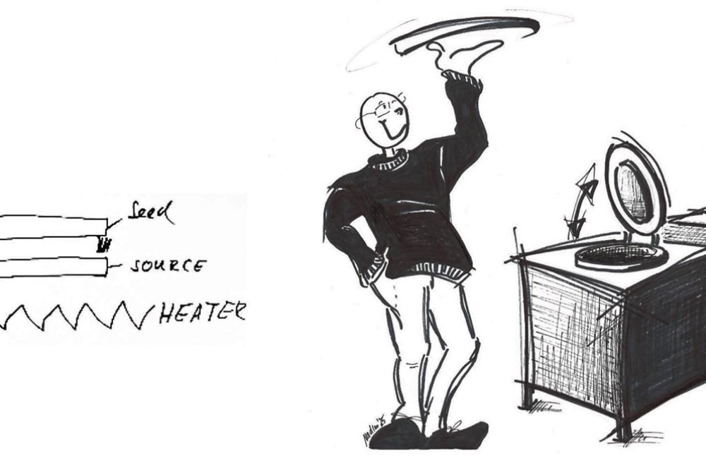
To help with this transition, our team at the University of Erlangen-Nürnberg (FAU) has developed a compact, table-top CS-PVT tool (see Figure 2). This versatile growth chamber can be easily integrated into a clean-room facility for device fabrication; deployed in a larger SiC wafer production line; and added to an academic research environment.

Figure 1. The evolution of standard PVT, prior to the introduction of CS-PVT.
What makes CS-PVT special?
Unlike standard PVT, which uses an inert gas for growth rate control, CS-PVT tends to employ vacuum conditions. Another key difference, which results from the geometrical design of the growth cell, is the opportunity to draw on much higher axial temperature gradients without having to alter the low radial temperature gradient. Thanks to this pair of levers, growth engineers can lower the growth temperature at the crystal growth interface – for example, reducing this from 2050 °C to 1900 °C – while maintaining the growth rate employed in standard PVT. Due to this, the crystalline quality realised by CS-PVT should be at least as good as standard PVT, and potentially even higher.
One feature of most CS-PVT tools is a spacer thickness of around just 1 mm between the crystal growth interface and the solid SiC source. This configuration, along with the vacuum environment and the comparably low growth temperature of around 1900 °C, creates a ballistic mass-transport regime. It’s a modus operandi that differs from that of standard PVT, where the gas phase resembles an ideal gas with Brownian molecular motion. With CS-PVT the SiC-based gas species – mainly silicon, Si2C and SiC2 – move from source to seed without interaction, preventing gas-phase reactions from taking place between gas species.
Crystal growth via ballistic mass transport is advantageous, offering favourable doping conditions for volatile dopants, such as the acceptor aluminium. In an ideal gas environment, aluminium would diffuse out, due to a higher partial pressure than the SiC-based gas species. Consequently, in the ballistic growth regime all acceptors are transferred from the sublimation surface to the crystallisation interface, enabling defined and high doping concentrations.
Today’s power electronics employs the so-called 4H-SiC polytype, which has a hexagonal crystal structure. That’s a shift from the early days of SiC development, when the focus lay on 3C-SiC, a polytype with a cubic crystal structure. As processing of bulk 3C-SiC turned out to be particularly challenging, 4H-SiC has been pursued as the SiC polytype for power electronics. However, this situation could revert, thanks to CS-PVT – it’s a growth technology that provides far higher axial gradients than its standard counterpart, and thanks to the lower growth temperature, growth conditions are favourable for stable crystallisation. While efforts surrounding
CS-PVT have been directed at high-quality, cost-efficient production of 4H-SiC, in future demand for 3C-SiC could be met by this growth technology.

Figure 2. Sketches of basic CS-PVT bottom heater concept (left) and
TableTopCS design (right) of the newly developed growth machine at FAU
dedicated to CS-PVT of SiC thick layers and bulk crystals.
A new CS-PVT tool
To fully exploit the benefits of the CS-PVT process, we have developed a new machine with characteristics that exploit the strengths of this growth process. Due to the flat design of the growth cell, we incorporate a bottom heater that heats up the system with the highest efficiency. Another strength of our design, which enables the growth of high-purity SiC layers, is an ultra-high vacuum (UHV) capability – we can reach vacuum levels as low as 10-8 mbar. What’s more, our system is a table-top set up (see Figure 2), so it can be easily integrated into a clean-room facility for device fabrication, or deployed in either a larger SiC wafer production line or an academic research environment.
Our initial results highlight the capability of our TableTopCS system for preparing thick single-crystalline layers of n-type 4H-SiC (see Figure 3, which depicts a 200 mm SiC substrate with a CS-PVT-deposited n-type layer with a thickness of around 150 µm). This layer has been grown at a rate of approximately 300 µm hr-1. We anticipate further process optimisation may lead to a reduction in growth rate to approximately 100 µm hr-1 to 150 µm hr-1, but this is still quite a high value.
Despite a source-to-seed distance of typically 1 mm or so, it’s possible to produce SiC crystals with a thickness of several millimetres with
CS-PVT. To accomplish this, during consumption of the solid SiC source, its top level must be lowered synchronously as the newly grown crystal extends its height downwards into free space. With this approach, the space between the SiC source and the newly grown SiC layer or crystal remains constant.
Using this methodology, we have grown SiC crystals with a thickness beyond 6 mm. While we are still to explore the technical limit of crystal thickness, a value of 10 mm should be feasible. However, what’s potentially difficult, from the point of process stability, is to reach a crystal boule height of 40 mm, a value obtainable in standard PVT.
Undercutting PVT?
Due to the potential reduction in boule height, when the CS-PVT process is employed for manufacturing SiC substrates, it requires three-to-four times as many boules as those produced by PVT to produce the same number of wafers. However, while growth rates are similar for both techniques, CS-PVT has a key advantage – far faster heating up and cooling down of the growth cell. This strength stems from the opportunity to undertake heat inflow and outflow during the heating up and cooling down steps, thanks to a minimum radial temperature gradient. The latter ensures that SiC crystal bending and cracking is unlikely in CS-PVT. Note, though, that it can be an issue in standard PVT. The upshot of all these factors is that the processing time for producing substrates by CS-PVT is roughly equal to that for PVT, and might be even shorter.
Another benefit that CS-PVT has over its conventional counterpart is a lower growth temperature. Moving from around 2050 °C to 1900°C delivers significant energy savings, as well as reducing the degradation rate of the applied graphite parts of the hot-zone.
There’s also the possibility of using multiple stacked growth crucibles during a single growth process. This opportunity for trimming costs strengthens the case that switching from PVT to CS-PVT will deliver a cost reduction in SiC substrate production.

Figure 3. Example of a 200 mm (∅196 mm) n-type 4H-SiC (4° offcut) CS-PVT layer on a 200 mm seed wafer.
Outperforming CVD?
Another opportunity for CS-PVT is to produce the thick intrinsic 4H-SiC drift layers, typically between 100 µm to 500 µm, that could lie at the heart of power electronic devices with blocking voltages above 3 kV.
Today, state-of-the-art intrinsic 4H-SiC layers for SiC power devices are formed by CVD, using growth temperatures of 1600 °C to 1700 °C and silane and propane precursors. Due to process instabilities, such as unintentional particle downfalls after long growth runs, drift-layer thickness is limited to 30 µm to 50 µm. Switching to CS-PVT removes this barrier, and a potential limiting factor, the purity of the drift layer. To investigate this opportunity, we are extending our exploration of CS-PVT to the epitaxial growth of intrinsic SiC layers, by equipping our new TableTopCS growth machine with a UHV capability.
Our upcoming efforts to exploit CS-PVT technology will also target the growth of SiC pucks in the several-millimetre thickness range, for the fabrication of 4H-SiC wafers; and the deposition of thin layers in the 100-300 µm range, for use in power electronic devices. A third development strategy will focus on the growth of SiC material in the 100 µm to 1 mm thickness range, for novel photonic applications, where special polytypes and dopants will be of interest.


