Korean team prints 'vertical nanolasers'
In a joint research team project with POSTECH (Pohang University of Science and Technology) the Korea Advanced Institute of Science and Technology (KAIST) has developed an ultra-fine 3D printing technology capable of creating 'vertical nanolasers' a key component for ultra-high-density optical integrated circuits.
Their paper 'Nanoprinting with Crystal Engineering for Perovskite Lasers' was published in ACS Nano in December 2025
Conventional semiconductor manufacturing methods, such as lithography, are effective for mass-producing identical structures but face limitations: the processes are complex and costly, making it difficult to freely change the shape or position of devices. Furthermore, most existing lasers are built as horizontal structures lying flat on a substrate, which consumes significant space and suffers from reduced efficiency due to light leakage into the substrate.
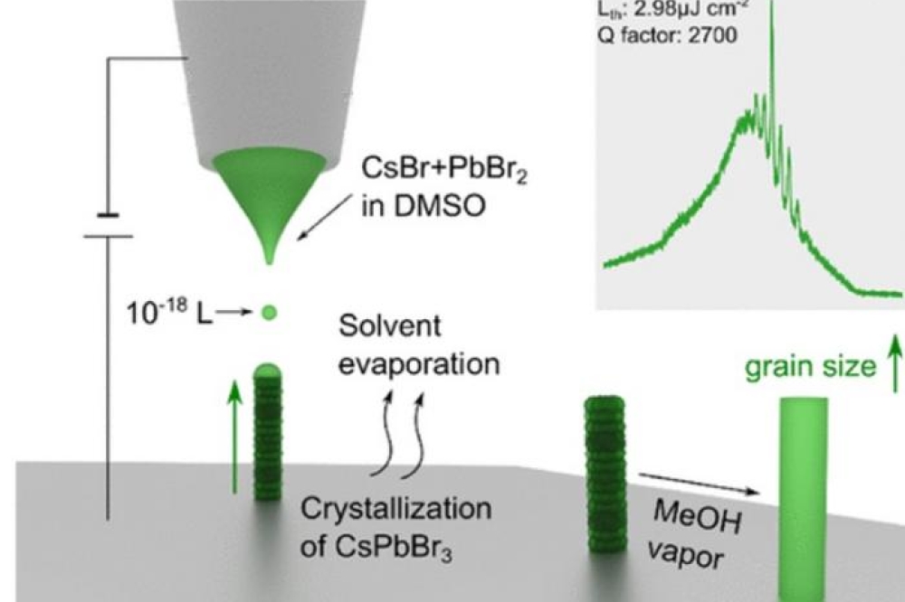
To solve these issues, the research team developed a new 3D printing method to vertically stack perovskite, a next-generation semiconductor material that generates light efficiently. This technology, known as 'ultra-fine electrohydrodynamic 3D printing' uses electrical voltage to precisely control invisible ink droplets..
Through this method, the team successfully printed pillar-shaped nanostructures—much thinner than a human hair—directly and vertically at desired locations without the need for complex subtractive processes (carving material away).
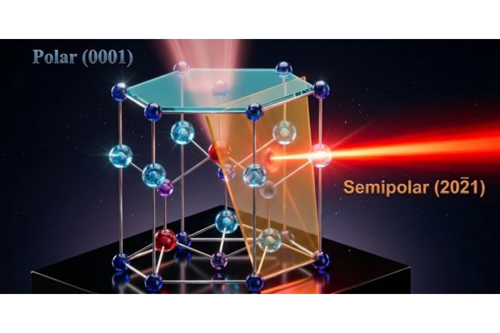
The core of this technology lies in significantly increasing laser efficiency by making the surface of the printed perovskite nanostructures extremely smooth. By combining the printing process with gas-phase crystallisation control technology, the team achieved high-quality structures with nearly single-crystalline alignment. As a result, they were able to realise high-efficiency vertical nanolasers that operate stably with minimal light loss.
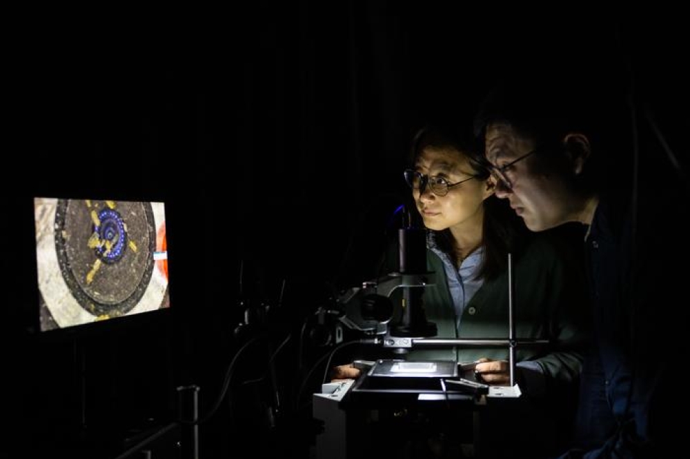
Additionally, the team demonstrated that the colour of the emitted laser light could be precisely tuned by adjusting the height of the nanostructures. Utilising this, they created laser security patterns invisible to the naked eye — identifiable only with specialised equipment—confirming the potential for commercialisation in anti-counterfeiting technology.
Project leader Ji Tae Kim, from KAIST's department of mechanical engineering said: "This technology allows for the direct, high-density implementation of optical computing semiconductors on a chip without complex processing. It will accelerate the commercialisation of ultra-high-speed optical computing and next-generation security technologies."

