6-inch InP fab begins construction in Eindhoven
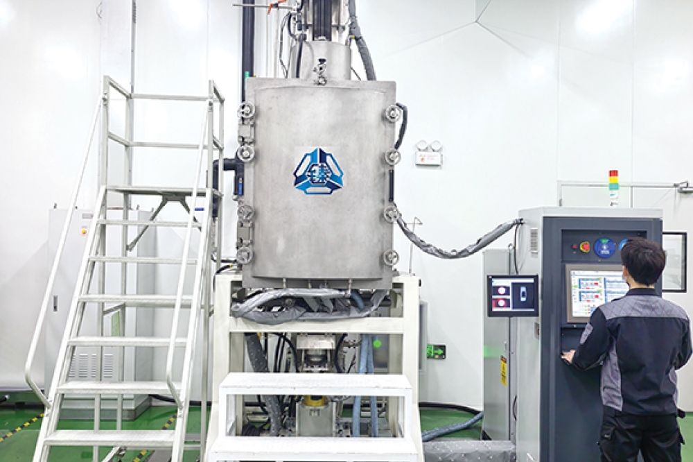
The Netherlands Organisation for Applied Scientific Research (TNO) and High Tech Campus Eindhoven are starting construction of foundry for producing InP photonic chips on a 6 inch wafer scale.
By connecting R&D with scalable production, the aim of this facility is to accelerate the path from concept to market-ready solutions for a new generation of energy-efficient AI data centres, 6G networks, medical innovations and supercomputers.
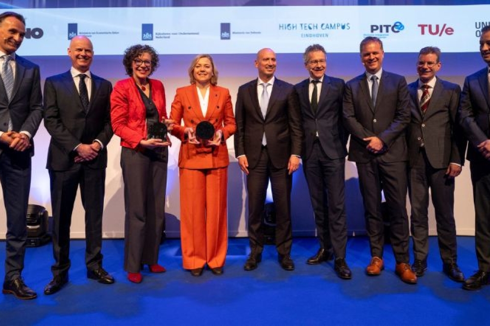
Tjark Tjin-A-Tsoi, CEO of TNO, said: "With this factory, TNO is taking a unique step: for the first time, we are building an industrial pilot line. By bringing research and manufacturing closer together, we strengthen the Netherlands’ position within the European semiconductor landscape and help companies scale up high-quality photonic technology more quickly and efficiently. This is an investment in our technological strength and in future economic growth.’
The €150 million investment stems from the ambition of the European Chips Act. As part of the pan-European consortium PIXEurope, the factory aims to ensure that the “brains” of the future digital economy are developed and produced on European soil.
The project is a public-private partnership between TNO, TU/e, PhotonDelta, SMART Photonics, and High Tech Campus Eindhoven. In addition to technological progress, the factory will create high-quality jobs. After the initial ramp-up phase, around 40 specialists will be employed at the factory, a number expected to grow further.
According to Netherlands government adviser Peter Wennink, the impact of integrated photonics is comparable to the rise of integrated electronics decades ago: "By investing now in scalable production capacity, we are creating an ecosystem that can help shape the global technological direction. This is a launchpad for Europe’s future digital economy."