

Study highlights integration benefits of micro-transfer printing
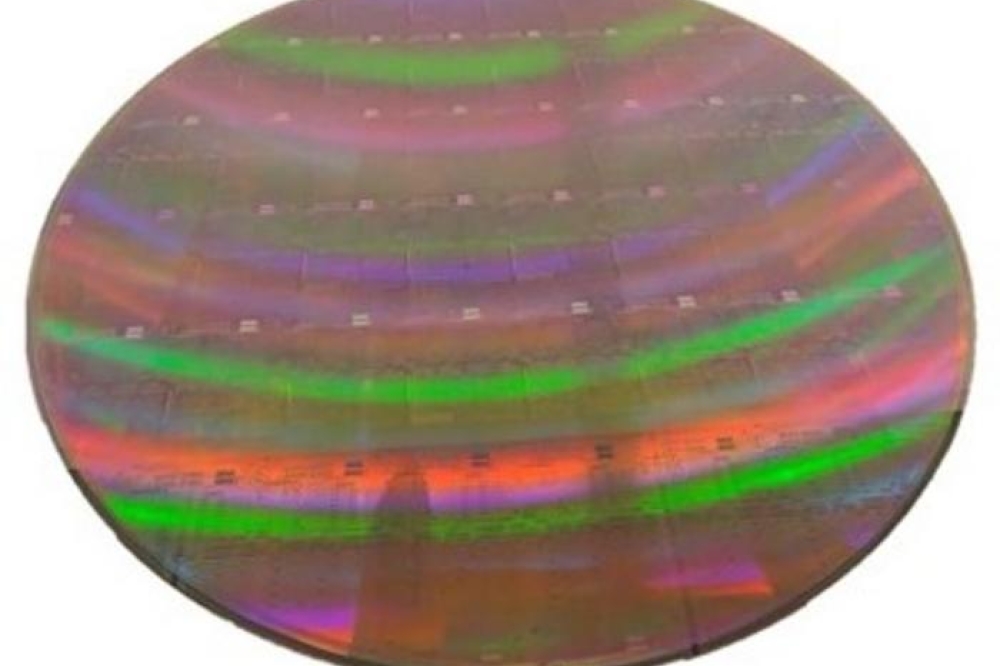
An IEEE study published in the Journal of Lightwave Technology on April 30, 2026, highlights micro-transfer printing (MTP) as a promising approach for realising heterogenous integration in silicon photonics.
“Among the various approaches being pursued for enabling wafer-scale heterogeneous integration, MTP is an emerging highly versatile technique that combines benefits of die-level assembly with wafer-scale processing,” explains Ye Chen from Ghent University, Imec, Belgium.
The study highlights the limitations of existing heterogeneous integration techniques before describing how MTP can address several of these challenges. The MTP process begins with fabrication of thin-film devices, called coupons, on a dense source wafer, followed by selective etching of a sacrificial release layer. An elastomeric stamp is then used to pick up and print multiple devices onto a target wafer. Finally, adhesive or direct bonding secures the devices in place, enabling seamless co-integration of diverse material systems onto large-area silicon photonics platforms.
Notably, one of the main advantages of MTP is its broad material compatibility, which allows multiple material systems to be integrated within a single architecture. This enables individual chiplets to be independently optimised using the most suitable fabrication processes before integration, while maintaining compatibility with CMOS-based photonic platforms.
Recent demonstrations of the MTP process include a fully integrated silicon photonic engine capable of processing both optical and microwave signals using InP lasers; GaAs lasers integrated with SiN waveguides for applications in virtual reality, quantum technologies and microwave photonics; widely tunable narrow-line width InP lasers integrated with silicon nitride (Si3N4) waveguides for coherent communications and light detection and ranging; wafer-level integration of LiNbO₃-based modulators with Si3N4 photonic circuits; and heterogeneous electronic-photonic optical receiver platforms.
The study also presents a new pilot line focused on developing key aspects of MTP for large-volume industrial manufacturing. In addition, the authors outline several remaining challenges, including yield, reliability, throughput, and the need for a robust and scalable manufacturing ecosystem, along with possible solutions for some of these issues.
“The MTP technology is still in its early stages of commercial application; however, we believe that consistent advancements will soon lead to large-scale industrial manufacturing, paving the way for advanced silicon photonics that will benefit several industries,” concludes Chen.



