

Precursor-modulated wells boost the efficiency of UVA LEDs
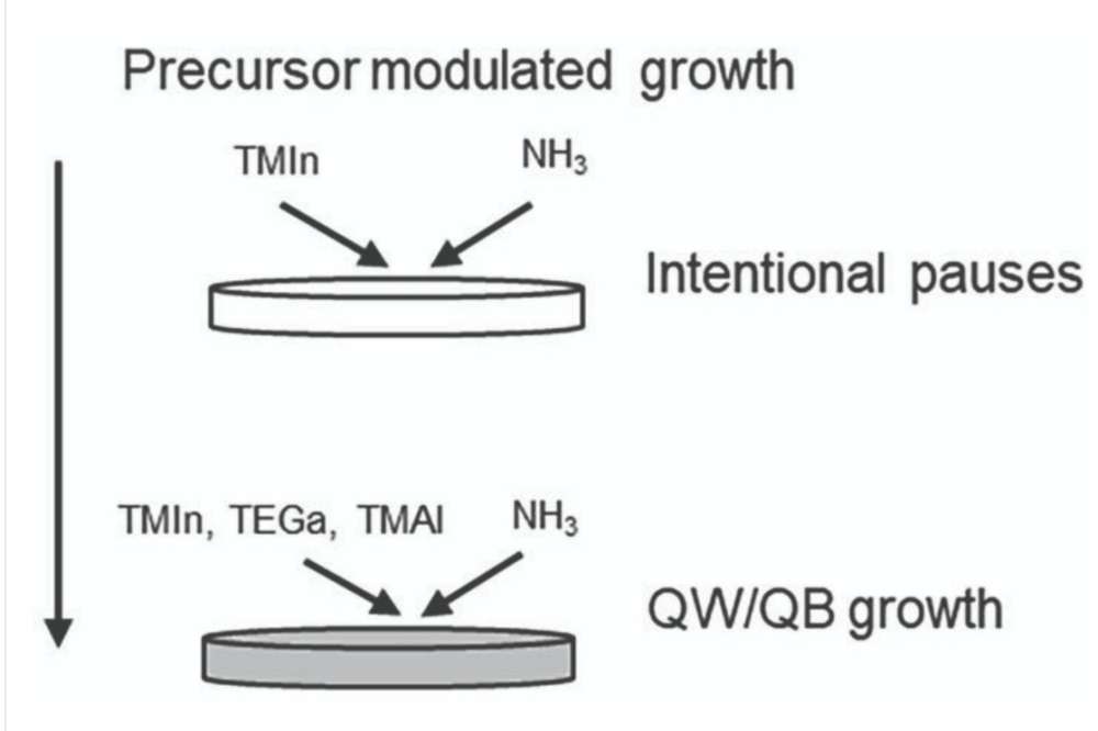
One weakness of LEDs emitting in the UVA – that’s the spectral domain from 315 nm to 400 nm – is the bandstructure, which features InGaN quantum wells with a relatively low indium composition, typically 5 percent. Due to this, offsets between conduction and valence bands are smaller than those in blue LEDs, leading to inferior carrier confinement. Compounding this issue, UVA LEDs are more sensitive than their blue-emitting cousins to interface quality.
To address both issues, the team from UCSB have drawn on earlier work involving AlGaN LEDs. “We found that the growth pause during the temperature ramp of quantum well growth could noticeably affect device performance, although the underlying mechanism was not fully understood at that stage,” remarks team spokesman Yifan Yao. “This motivated us to investigate the effect of precursor modulation more systematically in UVA LEDs.”
Yao and co-workers produced their devices by loading GaN-on-patterned-sapphire substrates into an MOCVD chamber and growing an epistructure featuring a 3 µm-thick n-type GaN buffer layer, a 200 nm-thick n-type Al0.06Ga0.94N layer, an active region with two quantum wells, a 15 nm-thick Al0.2Ga0.8N electron-blocking layer, a 300 nm-thick p-type Al0.06Ga0.94N layer, and a 15 nm-thick p-type contact layer.
When an active region is grown with a conventional approach, layers are deposited continuously, and there are no extended pauses. But in this work, there are intentional growth pauses. Between the growth of the well and the barrier there’s a pause for 8 minutes under a nitrogen gas ambient, with flows of just ammonia and a small amount of indium.
“The time was optimised for best device performance and repeatability,” remarks Yao. “We tried to pause for a shorter time, like 30 seconds or 1 minute, but this effect is less noticeable on device performance.”
During on-wafer electroluminescence measurements, the UVA LED with an active region grown with precursor modulation produced three times the output power of a reference device, grown conventionally. The more powerful device also supressed broad defect luminescence and had a narrower emission linewidth, thanks to improved carrier confinement.
To investigate the compositional fluctuations across the active region, the team employed scanning transmission electron microscopy energy-dispersive X-ray spectroscopy. This uncovered an aluminium-enriched interfacial layer, roughly 2 nm-thick, formed at well-barrier transitions. The team also produced top-emitting LEDs with sides ranging from 300 µm to 20 µm. Sidewalls were passivated by dielectric layers.
These devices exhibit a size-dependent droop that decreases with dimensions, due to reductions in localised heating and current crowding.
According to pulsed measurements with a 1 percent duty cycle, packaged 40 µm devices produce a peak external quantum efficiency above 41 percent, and maintain a value of 40 percent up to 200 A cm-2.
Yao says that the efficiency and the optical power of these devices are good enough for typical uses in many applications, including photolithography, curing, and photocatalysis.
Recently, the team applied its precursor modulation technology to the growth of laser diodes. This work will soon be published.
Reference
Y. Yao et al. Appl. Physical. Lett. 128 261109 (2026)



