
Breaking through the 10 kV barrier
Engineers from Novel Crystal, Japan, are claiming to have produced the first vertical Ga2O3 transistor with a blocking voltage of more than 10 kV.
According to the team, which produces the epitaxial layer of its device by HVPE, a switch in the growth plane from (001) to (011) is critical to their success. This move, supressing chlorine incorporation, enabled the formation of an epitaxial layer with a thickness of more than 50 µm and a donor concentration of less than 5 x 1015 cm-3.
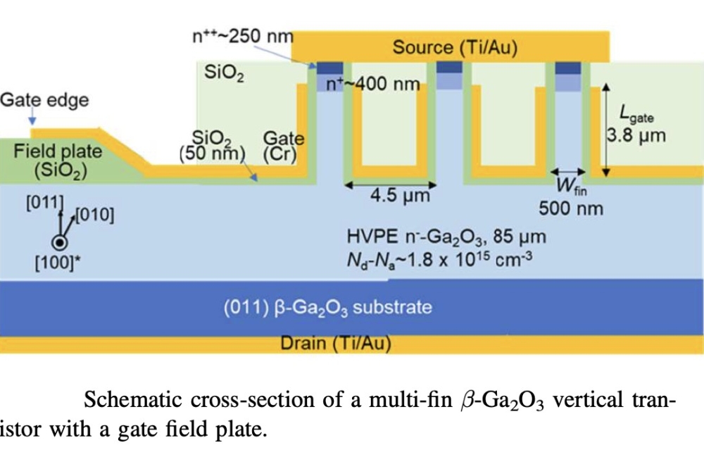
Fabrication of Novel Crystal’s multi-fin ß-Ga2O3 FETs began by loading heavily doped n-type (011) Ga2O3 substrates into a HVPE chamber and depositing a lightly doped n-type layer of 85 µm-thick Ga2O3. According to capacitance-doping measurements, the doping concentration in this epilayer is 1.8 x 1015 cm-3.
Silicon implantation and thermal diffusion, via annealing, produced a heavily doped n-type layer on the top of this film with a depth of 650 nm and a dopant concentration of around 1 x 1016 cm-3 to 8 x 1018 cm-3. Subsequent silicon implantation and activation annealing at 900 °C for 1 minute under nitrogen gas created a 200 nm-deep source contact layer with a silicon concentration of around 6 x 1019 cm-3.
The next steps of the fabrication process involved plasma-enhanced CVD of a layer of SiO2 and the patterning of chromium masks via electron-beam deposition and lithography, to define the size and location of the fin channels.
Dry etching, realising a near-vertical sidewall profile, defined the fin channels, prior to HF treatment for 15 minutes to remove the SiO2/chromium masks and the plasma-damaged layer.
To complete the multi-fin transistors (see figure for details of the structure), the engineers: employed plasma-enhanced CVD and atomic layer deposition to grow layers of SiO2; defined chromium masks, removed by dry etching; and added a Ti/Au source electrode on the fin top and a Ti/Au drain electrode on the backside of the substrate.
Novel Crystal’s engineers employed a scanning electron microscope to inspect their device, which has a fin width of 0.5 µm, a pitch of 5 µm, and a length of 70 µm.
The layout of the team’s device features 14 inner fins, surrounded by 4 outer fins. Of the 14 inner fins, 10 are covered with source electrodes and operate as the active layer of the multi-fin FET. With this layout, all fins under the source electrode exhibit the same FET characteristics.
One precaution taken by the engineers is to set the source electrode back from the fin edge by a few microns. This action prevents contact between gate and source electrodes at the deformed fin edge, an impairment caused by micro-loading effects during dry etching.
The team’s transistor, which has an active area of 45 µm by 70 µm, according to the arrangement of the source electrode and fin, has a maximum drain density of 15.1 kA cm-2 and a specific on-resistance of 289 mΩcm2 at a gate voltage of 3 V.
This device exhibits normally-off characteristics, with a threshold voltage of 0.68 V. Drain current on-off ratio exceeds 107, and the sub-threshold slope is around 77 mV dec-1.
To prevent early breakdown through air when conducting three-terminal off-state breakdown-voltage measurements, the team used a fluorinert solution. Testing revealed a blocking voltage in excess of 10 kV, the limit of the equipment, and enabled an estimation of the electric field at the centre of the trench of 2.55 MV cm-1.
Spokesman for the team, Daiki Wakimoto, told Compound Semiconductor they are now focusing on achieving a power figure-of-merit that exceeds that of SiC. Efforts will involve introducing an edge-termination structure that combines a magnesium guard ring and hetero p-type materials.
Reference
D. Wakimoto et al. Appl. Phys. Express 18 106502 (2025)


