Boosting the blocking voltage of birectional HEMTs
Engineers from the University of Wisconsin-Madison are claiming to have raised the bar for the breakdown voltage of monolithic bidirectional GaN HEMTs to 3 kV.
This class of device, providing bidirectional current and bidirectional blocking capability, is a promising candidate for a number of novel power converters – including matrix converters, multi-level T-type inverters, current source inverters and solid-state circuit breakers – that could increase the efficiency of renewable energy infrastructure.
Spokesman for the team from Wisconsin-Madison, Md Tahmidul Alam, told Compound Semiconductor that the conventional approach to realising bidirectional functionality involves two transistors and two diodes.
One downside of this approach is a high resistance, caused by contributions to overall resistance from multiple components.
Additional issues stemming from the high device count include increased complexity and a compromised reliability. “If any of the four components fails, the entire system does not work,” says Alam, adding: “Implementing the directional functionality with a single device reduces these complications.”
The team from Wisconsin-Madison claims to be the first to break the 2 kV barrier for monolithic bidirectional GaN HEMTs, with 3 kV devices with an on-resistance of around just 20 Ω mm. By breaking through the 2 kV barrier, the team’s devices are suitable for the construction of 1200 V class and 1700 V class power converters.
For power converters, normally-off transistors are preferred, as they can withstand accidental damage to the gate driving circuitry. While the team has used normally-on transistors in its latest work, these engineers argue that it is possible to apply similar concepts or designs to normally-off transistors when fabricating high-voltage devices.
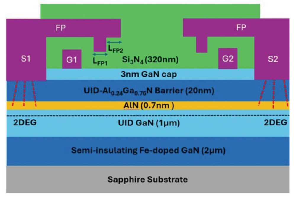
Production of monolithic bidirectional GaN HEMTs began by loading a sapphire substrate into an MOCVD reactor and depositing a 2 µm-thick semi-insulating layer of GaN, followed by a 1 µm-thick unintentionally doped layer of GaN, a 0.7 nm-thick layer of AlN, a 20 nm-thick Al0.24Ga0.76N barrier, and a 3 nm-thick GaN cap. The team selected sapphire over silicon for the substrate, so that they could reach blocking voltages beyond 2 kV.
Processing of the epiwafer into devices began by using lithography and metal deposition to form ohmic contacts. The next steps involved: a 750 nm deep mesa etch to isolate the devices; the addition of 200 nm-thick nickel gates; and surface passivation, realised by plasma-enhanced CVD of a 320 nm-thick layer of Si3N4.
The team produced a range of devices, differing in the lengths of the first and second field plates. The length of both of plates were varied from 1 µm to 3 µm.
Electrical measurements on the monolithic bidirectional HEMTs determined a stable threshold voltage of -3.25 V, a sub-threshold swing of 92 mV dec-1, and an on-off ratio of more than 105. According to the team, the stable threshold voltage, low sub-threshold swing and high on-off ratio makes their device suitable for high-frequency operation with low conduction and switching losses.
For most devices with a first field plate length no longer than 2 µm, the team recorded a breakdown voltage of 3 kV, the tool limit. But longer first field plates led to a lower breakdown voltage, possibly resulting from an increase in the electric field strength under the field plates that causes a high impact ionisation rate.
Pulsed current-voltage measurements up to a 40 V off-state switching voltage, using a 100 µs pulse width, have determined that current collapse is less than 10 percent.
One of the next goals is to increase the breakdown voltage and/or decrease on-resistance. Another aim is to measure the switching performance of the transistors at high-voltages, such as 600 V.
Reference
M. T. Alam et al. Appl. Phys. Express 18 016501 (2025)