
Sculpting at the micro-scale
Emerging fabrication techniques are re-writing the rulebook for on-chip components.
BY ARTHUR COLLIER, ABDALLA EBLABLA AND KHALED ELGAID FROM CARDIFF UNIVERSITY
From next-generation wireless to autonomous vehicles, there’s a race to higher frequencies that’s reshaping the demands on electronic hardware. At the heart of this pursuit is an urgent need for components that as well as being smaller and faster, are capable of handling the unforgiving realities of the millimetre-wave and sub-terahertz domain. At such high frequencies conventional fabrication methods struggle to fulfil these requirements, an issue that creates restrictions for designers trying to tackle the engineering challenges of next-generation systems. But progress is underway, with a new wave of innovation redefining the constraints for the design and fabrication of active and passive devices.
These advances are needed for emerging applications, which are increasingly pushing into millimetre-wave and sub-terahertz frequencies to access the wide bandwidths required. Such high frequencies demand low-loss, high-performance passive components, from filters and couplers to antennas and resonators.
In this high-frequency domain, GaN has established itself in active devices, due to its efficiency and high-power density. But it must be accompanied by surrounding passive structures, which must evolve just as quickly. In addition to addressing this goal, due to the drive for miniaturisation and system-in-package integration, there’s a need to develop highly compact passives with complex geometries that can be integrated monolithically. Here, the limitations of established methods for fabricating MMICs are becoming increasingly apparent.

Figure 1. Localised electrodeposition printing process control through laser deflection on a cantilever.
Until recently, conventional IC fabrication methods constrained the geometry of on-chip metallic structures. It’s a restriction that’s re-enforced by the IC design process, which ensures a planar approach, with layout files defined as sequential layers of two-dimensional shapes. Engineers have extended these methods to produce quasi-3D structures, such as air-bridges that allow circuit connections to cross one another. However, geometric freedom is severely limited by a reliance on temporary dielectric layers and resist chemicals as scaffolding during fabrication. Structures produced with this approach are constrained in span and height, with industry processes typically limited to just 1 µm - 2 µm above the substrate to maintain yield.
Breaking these shackles are recent advances in metal-additive micromanufacturing (mAM), which enable new possibilities in on-chip passive component design and fabrication. And within this new manufacturing technology is a particularly promising technique, localised electrodeposition, exemplified by commercial tools, such as the Exaddon CERES system. Localised electrodeposition enables highly conductive, fully three-dimensional structures with sub-micron feature sizes – an ideal platform for millimetre-wave passive components. Strengths of this form of localised deposition include its capability to produce, with sufficient reliability, complex geometries with horizontal and vertical aspect ratios of up to 100:1. The adoption of such methods in MMIC fabrication promises to rewrite the rulebook for millimetre-wave passive design and system-in-package integration.
Printing principles
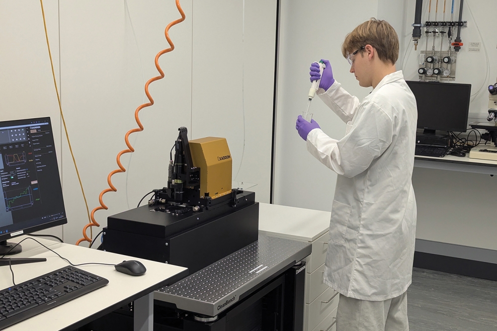
The operating principles of localised electrodeposition µAM are fundamentally different from those associated with conventional planar fabrication methods. Illustrating this point are tools such as the CERES µAM – employing a cantilever tip with a microfluidic channel, it delivers an aqueous solution that’s rich in metal ions directly to the intended site of electrodeposition (see Figure 1). The deposition occurs at the surface of a semiconductor sample, which must have either a metal seed layer or pre-existing metal features from prior fabrication. When using the CERES µAM, engineers place their samples in a chamber filled with electrolyte solution that provides a conductive medium between a potential applied at the sample surface and a counter electrode. The resulting electrochemical circuit ensures that electrodeposition take places, with microfluidic delivery through the cantilever providing the means to guide deposition to the desired location.
With localised electrodeposition µAM, a feedback mechanism must monitor the growth of each structure. Much like conventional 3D printing, designs are divided into individual voxels, which can be thought of as volumetric elements, representing the smallest unit of a 3D digital dataset. As each voxel forms, the deposited metal beneath the microfluidic nozzle causes the cantilever to bend upward. The tool detects this deflection using a laser, providing real-time confirmation of voxel completion. Once a voxel is finished, high-precision actuators reposition the stage in all three dimensions for the next voxel. Repeating this process enables the fabrication of arrays of on-chip passive components. Structures that have already been demonstrated range from helical antennas to shielded bond wires.
Possibilities for RF circuits
Our team at Cardiff University is able to access a recently installed µAM tool at The Institute for Compound Semiconductors. This new tool is a complimentary addition to this state-of-the-art nanofabrication facility.
Drawing on our GaN MMIC process, we have worked to extend its capabilities with the µAM tool, with the air-bridge stage quickly identified as a strong candidate for improvement. Air-bridges are essential in coplanar-waveguide MMICs – as well as enabling signals to cross, they preserve efficiency and signal integrity at impedance discontinuities. Critically to GaN technology, air-bridges are an attractive option for forming multi-finger transistors that ultimately allow devices to deliver the high-power-density devices that systems are demanding increasingly. While conventional air-bridges have helped engineers advance their MMICs, they have a major limitation, as they introduce parasitic effects on the coplanar waveguide beneath them.

Figure 2. Simulated scattering parameters of cavity waveguides,
illustrating improved matching and reduced insertion losses for taller
cavities.
To explore opportunities that might overcome this issue, our team has undertaken simulations that consider geometries well outside of the scope provided by conventional fabrication. By turning to µAM, we are able to construct air-bridges that reach greater heights, span wider gaps, and extend longer distances across waveguides. One design concept even enclosed an entire waveguide beneath a suspended cavity structure, effectively forming a ground plane above the coplanar waveguide – an idea that gave rise to the cavity coplanar waveguide.
We have found that the additional height provided by µAM is critical. Taller cavities improve matching and reduce insertion loss (see Figure 2). What’s more, we are able to engineer a null in the reflection coefficient, enabling enhanced matching within a specific bandwidth, with the null’s centre frequency tuneable through cavity geometry.
Voxels into structures
Following on from our device simulations, we have developed a process for printing an air-bridge using µAM. This structure comprises two supports and a connecting span – effectively three boxes, each built from individual voxels. To optimise the printing of these boxes, we balanced two key variables: the pitch, or spacing, between voxels; and the pressure applied during delivery of copper ions to the deposition site. For a fixed voxel pitch, we employed a higher pressure to improve filling and reduce gaps, but avoided the use of excessive pressure, as this causes voxels to merge, degrading print quality. We identified the optimal balance with test boxes, formed by varying pitch and pressure. Examining these boxes under a microscope revealed the optimal process, then used to construct the three boxes that are combined to form air-bridge or cavity structures.
Unfortunately, localised electrodeposition introduces challenges not seen in conventional 3D printing. One significant issue is that not all ions that exit the nozzle are deposited exactly where intended; some accumulate on nearby features – a phenomenon we call ‘spray deposition’. This unintended deposition must be factored into the design strategy. For example, if the first support is printed, followed by the second, prior to the connecting span, it’s critical to consider the spray that’s deposited on the first support during the second print as this alters its height. When returning to connect the span, this mismatch risks a tip crash. To avoid this, we leave an intentional small gap in the design, so the span can connect reliably without interference.
After taking these considerations into account, we printed final prototypes of an air-bridge and a cavity on a copper seed substrate. Scrutinising these structures with a scanning electron microscopy revealed impressive results: structures towering 50 µm above the surface – well beyond the limits of conventional air-bridge fabrication. Using optimised pressure, our voxels pitched 3 µm apart were densely packed, and provided seamless connections between the supports and span to yield robust, mechanically sound constructions.

Figure 3. Scanning electron microscope images of prototype air-bridge
and cavity with a height of 50 mm, printed on a copper seed substrate on
silicon.
Integration with circuits
Following these excellent printing results, we shifted our focus to implementation at the circuit level. These efforts involved the design of a planar layout, consisting of arrays of co-planar waveguides. We diced a 150 mm diameter GaN-on-SiC wafer into 25 mm by 25 mm tokens and employed photolithography to transfer the layout onto each token. Our next steps involved evaporating layers of titanium and gold, with titanium providing strong adhesion between the semiconductor surface and gold, before patterning a second resist layer to define the base positions of each bridge support. We have found that while not essential for printer operation, this resist pattern greatly improves optical alignment when positioning the printed structures on the existing waveguides. After patterning a second resit layer, we loaded the sample into the µAM tool for printing, with arrays of air-bridges and cavities aligned in a single step and printed sequentially. Finally, we removed the protective resist mask to reveal the finished sample.
Using these steps, we have printed a 50 µm-tall air-bridge on a co-planar waveguide that connects two ground planes (see Figure 4). When implemented at an impedance discontinuity, this electrical connection prevents parasitic modes, preserving signal integrity and efficiency. In our scanning electron microscopy image, shown in Figure 4, one can see dark rectangles at the base of the bridge supports, protruding above the gold waveguide surface. This observation indicates spray deposition through openings in the resist mask, which may additionally enhance adhesion of the air-bridge to the waveguide.
Performance potential
Scattering parameters are an essential tool for diagnosing the performance of RF components. Specifically for components that propagate signals within an IC, reflections of signal power may be indicative of poor impedance matching, and threaten to result in reductions in system efficiency, as well as posing a risk to signal integrity. As sensitivity to impedance matching becomes even more profound as operating frequencies push into the millimetre-wave and sub-terahertz domain, the reflection coefficient of interconnect structures is a very important parameter.
So how do co-planar waveguides with printed air-bridges or cavities perform in the millimetre-wave domain? To answer this, we turned to a vector network analyser to measure the reflection and transmission of signal power at each end of the co-planar waveguide. By sweeping frequencies from 1 GHz to 110 GHz, we covered the bands relevant to emerging and future wireless communications applications. Three devices were characterised: a bare co-planar waveguide; and variants with an air-bridge and a cavity.

Figure 4. Scanning electron microscopy image of a printed air-bridge aligned to a co-planar waveguide on a GaN-on-SiC substrate.
Our results show that transitioning from the air-bridge to a cavity covering the co-planar waveguide increased reflection and transmission coefficients across the entire measured frequency range. At 110 GHz, the reflection coefficient increased by 35 percent without compromising insertion loss. Another encouraging experimental result is that we observed the wide-bandwidth null in reflection coefficient predicted by simulations, a finding that highlights the potential for engineered matching within a specific bandwidth. Simulations also indicate that the position of this null is proportional to cavity dimensions, suggesting that careful design of the cavity geometry could enable tuneable performance in future devices.
To conclude, we have successfully integrated our µAM process into our GaN MMIC fabrication workflow, to demonstrate significantly enhanced geometries attainable for passive structures. Notable triumphs within this work include: the construction of air-bridges spanning 50 µm above the surface, far exceeding the limits of conventional fabrication methods; and an initial exploration of co-planar waveguides enclosed within a cavity, a study that reveals the potential for improved matching at impedance discontinuities in the millimetre-wave domain.

Figure 5. Scattering parameters comparing a bare co-planar waveguide
(CPW), a CPW with a printed air-bridge, and a CPW with a printed cavity.
The development of µAM to advance the fabrication capabilities of active and passive components marks a new era in the way we consider both the design and the fabrication of millimetre-wave wave ICs. There is good reason to believe that metal additive micromanufacturing can play a pivotal role in delivering the intricate structures required by miniaturisation and system-in-package integration. Our demonstration of localised electrodeposition µAM within the GaN MMIC process represents a key step toward implementations that could redefine the performance potential of millimetre-wave applications.
The authors would like to thank Exaddon AG for their technical support and IQE PLC for provision of GaN epitaxial material support. We would like to acknowledge the Institute for Compound Semiconductors (ICS) for usage of their facilities.


