
Advancing Ga₂O₃ diodes with copper anodes
Engineers from China are claiming to have delivered a significant advancement in the performance of b-Ga2O3 power rectifiers through the introduction of copper anodes.
According to the spokesman for the team, Xiaohui Wang from Southern University of Science and Technology, by integrating a Cu2O/Ga2O3 heterojunction with a low work-function copper anode, this collaboration has produced a diode that combines a turn-on voltage of less than a volt with a breakdown voltage beyond 2 kV. The result is a leading figure-of-merit for power devices.
Another feature of this device (produced by a partnership involving researchers at Southern University of Science and Technology, Peng Chen Laboratory, The University of Hong Kong and Shenzhen Polytechnic University) is its enhanced field control.
It is said that the highly doped p-Cu2O layer and the Cu2O-based junction termination extension effectively redistribute the electric field and suppress peak electric field crowding. According to Wang, these breakthroughs have played a key role in establishing a new material platform and design strategy beyond conventional NiO/Ga2O3 heterojunction barrier Schottky diode structures.
Wang and co-workers are not the first to try and improve NiO/Ga2O3 by turning to Cu2O, an alternative that helps to excel on two key fronts: a high blocking voltage and a low forward voltage. Previous success has been reported by engineers at NCT, producing an ampere-class large-area diode that’s optimised for high current density and switching performance.
“Our work introduces a low work-function copper anode with an in-situ platinum layer to form an optimised p-contact to copper oxide,” explains Wang, who points out that the device from NCT, featuring nickel contacts and produced using a lift-off trench-filling Cu2O process, has significantly higher values for on-voltage and specific on-resistance.
Another strength of the device produced by the team from China is a result of its optimised planar p-Cu2O ring, which suppresses electric-field crowding and shifts the peak electric field into the drift region.
Efforts by Wang and co-workers have not been restricted to device design, and include the fabrication process: “Our device benefits from rigorous interface engineering, including copper oxide with a high hole concentration, an in-situ platinum contact and surface preparation. These processes lead to lower leakage, a more uniform electric field distribution, and superior thermal/electrical reliability.”
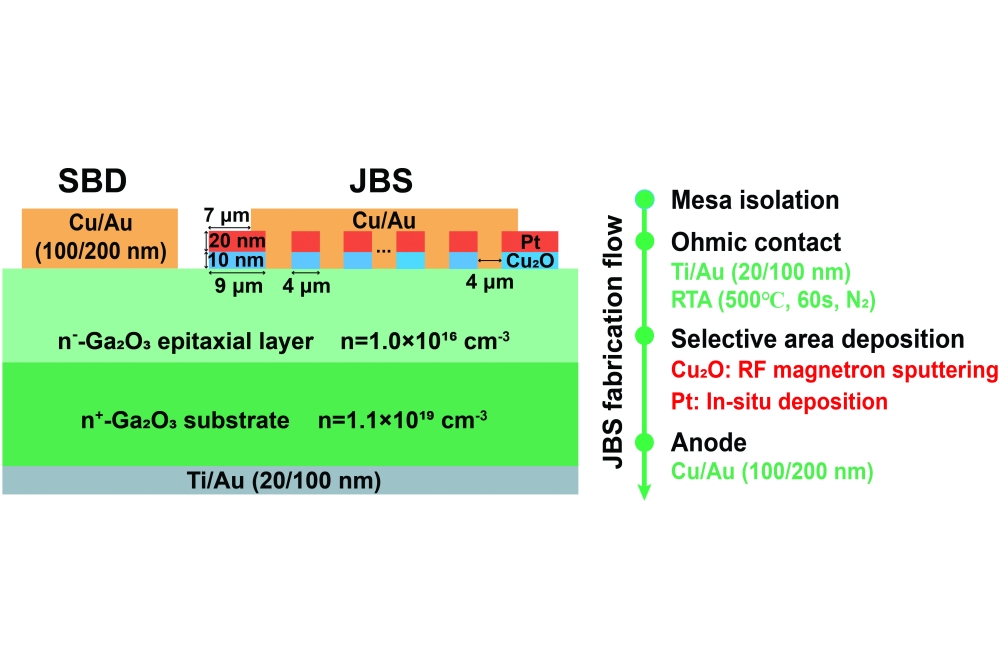
Devices have been produced by processing epiwafers, featuring a 10 µm-thick silicon-doped drift layer on a heavily tin-doped native substrate, into Schottky barrier diodes and heterojunction barrier Schottky diodes (see Figure for details).Characterisation of the latter determined a turn-on voltage of 0.83 V, a breakdown voltage of 2345 V, and a figure-of-merit for power of 1.22 GW cm-2.
Efforts have also been directed at evaluating long-term reliability. Operating under a 200 V reverse-bias stress at 425 K for 10,000 s produced negligible degradation in dynamic on-resistance and on-voltage. “Combined with a trap-related mechanism analysis, these results offer critical experimental evidence for the practical deployment of gallium oxide devices in high-temperature, high-voltage applications,” argues Wang.
One of the team’s goals is to improve heterojunction quality through a combination of controlled oxidation, refined surface treatment, and alternative deposition strategies.
“These efforts are expected to suppress interface trap density, enhance carrier transport uniformity, and further reduce leakage and barrier inhomogeneity,” says Wang.
There are also plans to: increase the breakdown voltage while maintaining the low specific on-resistance of 4.5 mΩ cm2, a goal that will be pursued by introducing either multi-zone junction termination extension, field plates, or hybrid termination structures; and to explore the on-chip integration of the team’s diodes, by using surge-protection devices, field-control components, and high-voltage rectifiers.
Pictured above: Schottky barrier diodes (SBDs) and heterojunction barrier Schottky diodes (JBSs) benefit from a highly doped p-Cu2O layer and a Cu2O-based junction termination extension.
Reference
X. Wang et al. Appl. Phys. Lett. 127 212102 (2025)


