
Navitas unveils 5th gen SiC technology
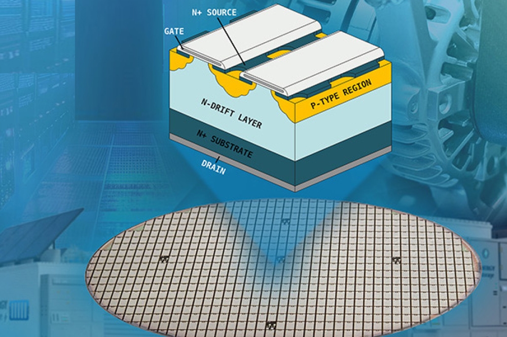
Navitas has announced the launch of its 5th-generation GeneSiC technology platform. The High Voltage (HV) SiC Trench-Assisted Planar (TAP) MOSFET technology is claimed to represent a significant technological leap over previous generations.
The technology, which will be used to make 1200V devices, complements Navitas’ ultra-high voltage (UHV) 2300 V and 3300 V technologies from the 4th generation GeneSiC platform.
The 5th generation MOSFET platform features Navitas’ most compact TAP architecture yet, combining the ruggedness of a planar gate with high performance enabled by a trench structure in the source region while also elevating the efficiency and life-time reliability for high-voltage power electronics.
The 5th generation platform is said to achieves a new benchmark in power conversion through a 35 percent improved RDS,ON × QGD figure of merit (FoM), as compared to the previous generation 1200 V technology. This improvement slashes switching losses, allowing for cooler operation and higher frequency of operation in demanding power stages.
High-speed switching is further fortified by ~25 percent improvement to the QGD / QGS ratio. When paired with a stable high threshold voltage specification (VGS,TH ≥ 3V), this technology ensures immunity against parasitic turn-on, providing a robust and predictable gate drive even in high-noise environments.
The 5th generation technology delivers improvement in dynamic performance by optimising the RDS(ON) × EOSS characteristic while also integrating a 'Soft Body-Diode' technology to further enhance system stability by minimising electromagnetic interference (EMI) and ensuring smoother commutation during high-speed switching cycles.
AEC-Plus grade qualification of this generation ensures long-term stability and durability for AI data centres, energy and grid infrastructure applications.
Key reliability benchmarks include: 3x longer duration for static high-temperature, high-voltage testing (HTRB, HTGB, and HTGB-R); dynamic reverse bias (DRB) and dynamic gate switching (DGS) to represent stringent fast-switching application mission-profiles; and extrapolated gate-oxide failure time exceeding 1 million years at operating VGS at 18V and 175°C.
The technology also has enhanced cosmic ray resilience with low FIT (Failure In Time) rates, ensuring mission-critical reliability in high-altitude and high-uptime environments.
“Our customers are redefining the boundaries of power conversion in AI data centres and energy infrastructure, and Navitas is marching along with them in every step of the way,” said Paul Wheeler, VP & GM of Navitas’ SiC Business Unit. He added, “significant technological improvements in our 5th generation GeneSiC technology underscore Navitas’ commitment to delivering industry-leading performance and reliability in silicon carbide MOSFETs.”


