Aiding AI with the microLED
Promising to provide the most efficient links for tomorrow’s energy-hungry data centres are links formed from vast arrays of microLEDs, employed alongside optical fibres and photodetectors.
BY RICHARD STEVENSON, EDITOR, CS MAGAZINE
Around the turn of the millennium many bought their first mobile phone, a purchase that helped to swell revenues for our industry on two different fronts. Sales created the first ‘killer’ application for the LED, coming from backlighting the displays and keypads of these handsets, and it led to rocketing revenue of GaAs HBTs and pHEMTs, with these devices deployed in RF amplifiers and switches.
Since then, there’s not been another application that’s delivered multi-billion-dollar sales for more than one class of device within the compound semiconductor industry. But that could change, thanks to AI, which is fuelling a hike in the roll-out of data centres. Many makers of wide bandgap power devices are saying that they are aiming to exploit growth in data centres – efforts are directed at securing contracts for discrete components and modules for electrical infrastructure that combine exceptional efficiencies with the handling of high power densities. But there’s also an opportunity within the optoelectronics sector, for sources and detectors that can form short-reach optical links that overcome a data transfer bottleneck while minimising the energy-per-bit.
Focusing on the latter is a three-year project starting this January. Led by French technology research institute CEA-Leti, this effort aims to drive the development of optical links formed by combining arrays of GaN-on-silicon microLEDs with fibres that have a relatively wide core and photodetectors. It is intended that this project will involve all the key players in the supply chain, including manufacturers of microLEDs, optical fibres, photodiodes and interconnects, as well as chipmakers, system integrators, and hyperscalers.

Working principle of microLED based Data Link Credit: Patrick Le Maitre, CEA
According to Jankus Vygintas, CEA-Leti Partnership Manager spokesman for this three-year project – it’s referred to as the Multilateral MicroLED Data Link Program – the proposed optical links could be deployed to transfer data from one chip to another within a board, or from one chip on one board to one chip on another board. Chip-to-chip transfer could even go from server to server or rack to rack, as the technology offers much appeal for links spanning 10 cm to 10 m.
Note that Vygintas is not suggesting the complete elimination of copper in data centres, arguing that this is the best choice for distances of just a few centimetres. But this should be the upper limit, as the longer these wires get, the more energy they consume.
Giving the success VCSELs have had in datacomms, they are another candidate for chip-to-chip links.
“For pluggables and so on, for longer distance links, it's probably the best developed technology” claims Vygintas, who explains that this surface-emitting laser can be viewed as a ‘Ferrari’ for short links, from both a cost and an efficiency perspective.
Providing a starting point for the project is the significant body of microLED work conducted by CEA-Leti that’s led to the generation of around 100 patents. The well-renowned French research institute has been developing microLEDs since at least 2015, and around six years ago its efforts started to involve the modulation of these devices, initially to gauge their potential as sources for LiFi.
More recently, the focus has shifted to coupling the emission from microLEDs into fibres, and evaluating a key metric, the picojoules-per-bit.
“Nowadays, we are at around 5 picojoules-per-bit,” reveals Vygintas, who adds that a primary objective of the project is to slash this critical figure to just 0.5 picojoules-per-bit.
“The other target is, of course, data density. In the long term, we aim to reach 10 terabit per second per millimetre.”
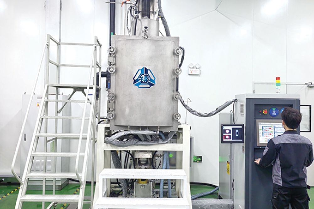
In CEA-Leti’s 11,000 m2 cleanroom researchers have developed a process for producing GaN-on-silicon LEDs on 200 mm substrates. Note, though, that the process can be scaled to 300 mm.
The team can shrink the size of its microLEDs to just a few microns – dimensions that are ideal for augmented reality, but a level of miniaturisation that introduce issues, including quenching at the edges of these emitters. For short-reach data links, Vygintas recommends using microLEDs with a size of around 10 µm, with emission coupled into fibres with a core of around 50 µm.
“We work on emission in the blue, but in principle, emission in green or red would be possible,” says Vygintas.

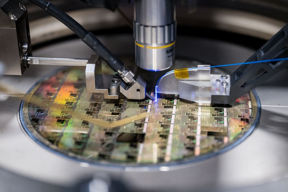
An example of a microLED array, which measures approximately 300
micrometers in diameter. Copyright: CEA-Leti, Patrick Le Maitre
While at first glance shifting emission to longer wavelengths is deleterious, driving a decline in efficiency that stems from an increase in indium content in the quantum wells, this view fails to grasp the bigger picture. That’s because many more factors are at play, such as modulation bandwidth, fibre coupling and losses, and the efficiency of the detector – all contribute to the key metrics.
For data links, the emission from arrays of microLEDs is coupled into fibre bundles, a technology already employed for imaging in medical applications.
“We are testing all type of fibres, including plastic fibres,” reveals Vygintas. “Some manufacturers provide glass multi-core fibres.”
A key advantage coming from combining arrays of microLEDs with fibre bundles is a built-in redundancy at the system level.
“The VCSEL has to be well aligned, but in our case, we can afford some loss,” claims Vygintas, who explains that the team at CEA-Leti tackles this task with partners that fabricate alignment and attach tools for the silicon photonics industry. These collaborators can use their technology to attach fibres to microLEDs.
Vygintas believes that an even better approach involves refining the design of the microLED so that it includes a resonant cavity that creates an emission profile tailored to coupling into a fibre. Such a device demands the introduction of Bragg mirrors made from dielectrics.
One of the options for the detector that’s positioned at the other end of the fibre is a silicon-based diode, which is a well-established device; and the other contender is a GaN photodetector. While the latter is inferior today, it has a reasonable responsivity, and would simplify device integration. To try and improve performance, the team at CEA Leti are aiming to optimise the epitaxial process for producing these devices.
Thanks to the fabrication of devices on silicon, drivers for these microLEDs can be added by bonding to the backplane. Over the last four years Vygintas and co-workers have adopted this approach when they’ve been comparing various modulation schemes. While the more complicated ones may have greater promise, the team has concluded that the best solution is a basic on-off modulation scheme that simplifies amplification and photodetection.
“It should also be more efficient, because higher modulations can consume more energy,” adds Vygintas.
He believes that CEA-Leti’s status as a research institute ensures that it’s in a great position to nurture the formation of an ecosystem for producing microLED-based short-reach optical links. Over the next three years, they will be bringing together those working in the lighting, semiconductor and fibre industries from all around the world. Some of these companies are already on-board – but their names cannot be revealed, due to non-disclosure agreements – and many more are expected to join.
“We occupy very special place in the whole ecosystem to provide prototypes. We are open to discussions with everybody,” says Vygintas.
By adopting such a collaborative stance, CEA-Leti is giving the microLED a great opportunity to find its first killer application, and increase compound semiconductor content in the data centres of tomorrow.