
Driving the electric revolution with SiC IGBTs
FOR2ENSICS, an EU-funded initiative, is targeting the simplification of medium-voltage DC converters with ultra-high-voltage SiC IGBTs.
BY NAZARENO DONATO, UNIVERSITY OF CAMBRIDGE
The global drive to trim carbon emissions and reach climate neutrality is rapidly transforming electricity supply and grid infrastructure. Critical to succeeding in this endeavour is the introduction of a new generation of power devices, delivering higher efficiencies at reduced costs, through a smart combination of reduced epitaxial layer thickness and a smaller form factor.
One promising route towards this goal is DC distribution, well matched to renewable sources and modern loads, such as solar arrays and battery systems, which already operate in DC. But the power electronics market still lacks low-cost, compact, high-performance DC-to-DC converters that are capable of handling voltages from below 1.5 kV to well over 10 kV.

Figure 1. Schematic process flow for the fabrication of ultra-high-voltage SiC IGBTs.
Aiming to close that gap with a commercial-grade DC-to-DC converter featuring a medium-voltage stage based on ultra-high-voltage SiC IGBTs is our Horizon Europe-funded project entitled Future Oriented Renewable and Reliable Energy SiC Solutions (FOR²ENSICS). By turning from series-connected medium voltage (1.2 kV - 6.5 kV) SiC MOSFETs or silicon IGBTs to ultra-high-voltage SiC IGBTs, we promise to unleash a number of key benefits, including lower conduction losses, simpler drive requirements, a smaller footprint and reduced costs. However, delivering such technology demands coordinated expertise in device fabrication, passivation, packaging and converter assembly – goals realised by a joint effort, drawing on a broad range of expertise from industry and academia.
SiC IGBT technology
Silicon-based IGBTs have long been a mainstay in traction, industrial, automotive and high-voltage DC systems, typically operating from 900 V to 6.5 kV. Their bipolar conduction helps overcome MOSFET limitations, improving the trade-off between the static voltage drop and turn-off losses.
With the arrival of 4H-SiC unipolar devices in the 1.2 kV -3.3 kV range, silicon IGBTs – still extremely cost-competitive – are losing ground in medium-voltage applications. However, for 6.5 kV and beyond, SiC MOSFETs are up against scaling and cost limits, even with superjunction concepts. On one hand, yield and defect density limit the maximum achievable die area; on the other, scaling of the drift region resistance makes the SiC MOSFET less suitable for medium- to high-current applications.
For ultra-high-voltage applications – that’s more than 10 kV – operating at moderate switching frequencies of tens to hundreds of kilohertz, the SiC IGBT offers a compelling alternative. Its advantages include avoiding some of the drawbacks of series-connected SiC MOSFETs, which are more susceptible to voltage imbalance and require more complex gate driving. In addition, SiC IGBTs benefit from a reduced drift-region thickness, compared with their silicon siblings. This gives the SiC IGBT a fundamental advantage, resulting from a lowering of stored charge that ensures reduced switching losses.
Enjoying the benefits of the SiC IGBT is not easy, as its design brings significant challenges, due to intrinsic material constraints. One issue is the higher forward voltage drop, stemming from a delayed bipolar turn-on. This drop – measured at room temperature it’s 2.8 V for 4H-SiC, versus 0.7 V for silicon – leads to increased conduction losses at low and medium currents. The other noteworthy drawback is the limited minority-carrier lifetime – only recently extended into the microsecond range – that reduces the benefits of bipolar conduction when the diffusion length is smaller than the drift region thickness. The peak minority-carrier lifetime achieved in the last ten years also limits the maximum drift-region thickness between 100 µm to 200 µm, placing the optimal performance window between 10 kV and 20 kV – the target range for our FOR²ENSICS project.

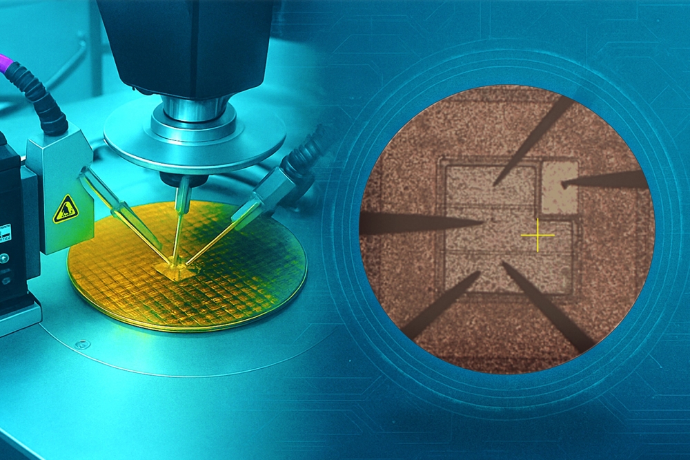
Figure 2. (a) IGBT characteristics prior to thick metal deposition and
(b) a microscopic image of the IGBT under test in the Henry Royce High
Voltage Characterisation Suite (Cambridge University).
The backside processing conundrum
Manufacturing n-type SiC IGBTs for ultra-high-voltage applications is a non-trivial task. Challenges arise, due to the absence of high-quality p-type SiC substrates, and the need for thick, high-quality epitaxial layers to support blocking voltages beyond 10 kV. In recent years, researchers have explored different fabrication routes, like the flip-type process – this involves removing the n+ substrate and forming the device channel and the gate oxide on the carbon face – alongside careful process and design optimisation. However, this promising route is yet to yield a commercial SiC IGBT, largely due to cost and performance constraints (as well as mechanical stability).
Our project is pursuing a more streamlined approach, which retains the thick epitaxial layer and substrate throughout processing. Starting with an n+ substrate, our flow involves forming a highly doped p-type collector, adding a buffer layer, growing the epi, and then fabricating the top MOS cell. Backend processing includes substrate splitting or removal – using a combination of back grinding, chemical mechanical polishing and etching – to enable either reuse of the substrate (laser cut achieved through Kabra split or similar methods) or backside access (see Figure 1), prior to metallisation.
Early trials have delivered encouraging results, indicating that our approach is a viable manufacturing route. Our first batch of SiC IGBT devices is currently under test, with preliminary results show promising gate modulation and successful backside substrate removal (see Figure 2).
In parallel, we are producing SiC MOSFETs rated at 3.3 kV, 10 kV and 15 kV to benchmark against our IGBTs in a DC-to-DC converter dual-active-bridge demonstrator.
Leading this high-voltage SiC device fabrication effort are our consortium members at The University of Cambridge, Coherent, CNM and Hitachi Energy.

Figure 3. (a) Photo of 10 kV SiC MOSFET wafer and (b) wafer-level
forward-blocking characteristics for MOSFETs implementing D3 termination
design, measured at room temperature with a gate-source voltage of
zero.
Edge termination design
For ultra-high-voltage SiC devices with ratings above 10 kV, it is critical to employ an efficient edge termination. Conventional termination designs capable of withstanding such voltages tend to require large die areas – and that’s a costly design solution when working with epiwafers over 100 µm-thick that must deliver tens of Amps. The aim is to minimise the termination footprint while maintaining robust blocking performance and avoiding any compromise to passivation and oxide reliability.
Testing of a SiC MOSFET platform has already demonstrated edge terminations capable of blocking more than 10 kV during on-wafer measurements (see Figure 3). We have also developed a new test platform for packaged devices that evaluates up to 20 kV, along with a double-pulse test system operating above 10 kV using a dedicated DC supply. The next stage is to prove these termination concepts on IGBTs.
Packaging and reliability
To unlock the full potential of high-voltage SiC technology, packaging must combine electrical performance with long-term reliability at 15 kV. Our package design uses high-field passivation and gel materials to withstand extreme voltages, temperatures and humidity without degrading device performance. This package supports both the integration of high-voltage SiC MOSFETs and IGBTs (in parallel or series connection) with a high-voltage SiC diode – a MOSFET in diode mode – providing wide flexibility for all the devices manufactured within the project.
A PCB mezzanine within the module carries integrated passive components, such as gate driver resistors, a negative-temperature-coefficient sensor and an RC snubber (see Figure 4 (a)). Leading this work are Deep Concept and the SuperGrid Institute.
We have used a number of standard approaches to evaluate reliability. They include high-temperature reverse-bias tests, investigation of time-dependent dielectric breakdown and the high-humidity, high-temperature and high-voltage reverse-bias test. Results confirm the robustness of our high-voltage SiC IGBTs. In addition, there’s a multi-die test platform for bipolar degradation studies – capable of testing up to 16 devices in parallel – that’s now operational at the University of Bremen.

Figure 4. (a) Ultra- high voltage packaging concept for SiC IGBT and (b) dual active bridge demonstrator.
Gate drivers and converters
A major demonstration target for our project is the dual-active-bridge converter, selected for its efficiency and adaptability in medium-voltage DC applications. The first prototype, showcased this November at the SuperGrid Institute in Lyon, uses a series-connected 3.3 kV SiC MOSFET (see Figure 4 (b)). This platform serves as our baseline for a follow-up demonstrator in 2026, using the project’s 15 kV SiC IGBTs.
Our single-phase dual-active-bridge converter comprises two full bridges – one connected to the low-voltage bus, designed with LinPak SiC MOSFETs from Hitachi Energy; and the other to the medium-voltage bus – linked through a medium-frequency transformer. The converter benefits from the opportunity to operate at elevated switching frequencies of tens of kilohertz, because it is not tied to the grid’s 50/60 Hz. Thanks to this freedom, the convertor can operate at a higher power density and be constructed from smaller passive components.
Moving to ultra-high-voltage SiC devices on the medium-voltage side also demands advanced gate driver technology. As well as translating control signals into required drive levels, the driver has to handle short-circuit events, limit over-voltage, and employ active Miller clamping to avoid parasitic turn-on. For series-connected switches, it’s also critical to ensure precise voltage sharing during static and dynamic conditions. Fulfilling all these requirements enables the design to integrate voltage-balancing measures alongside tuned gate resistances. Leading this work are EPFL and the SuperGrid Institute.
Features of our dual-active-bridge converter include galvanic isolation of the gate driver’s power supply, employed to withstand high common-mode transients, and a layout that’s optimised to minimise parasitics that could impair superior switching performance. Together, these design choices ensure that the converter exploits the high efficiency and robustness of ultra-high-voltage SiC devices, and provides a strong platform for validating SiC IGBTs in demanding medium-voltage DC systems.
Next steps
As the project enters its core phase, with new IGBT devices emerging from the fab and packaging activities underway, our consortium is moving into a more mature stage of development. Our recent research efforts have focused on making additional improvements to backside metallisation contact resistance and substrate removal, as well as developing multi-die packaging solutions – connecting up to four devices in parallel – to meet the higher current requirements of the final dual-active-bridge demonstrator. We are also progressing modelling and simulation activities in parallel, efforts that will help enhance IGBT performance in upcoming batches, particularly in terms of current capability and temperature coefficient.
Successful proof-of-concept demonstrations at both the device and system levels have encouraged our consortium to pursue new ideas. They include: advanced device concepts, such as reverse-conducting SiC IGBTs; further reductions in the edge termination footprint; novel packaging approaches, using ultra-high-field-strength passivation materials; and the development of larger active areas, as yields continue to improve. If you want to say informed, follow the project updates on our website and social media platforms.
FOR2ENSICS has received funding from the European Union’s Horizon Europe research and innovation programme under grant agreement No 101075672.


