
Scientists solve 2D semiconductor mystery
So far finding and developing 2D semiconductor materials has been largely down to trial and error. Now research by scientists at Trinity College Dublin’s School of Physics and AMBER, the Research Ireland Centre for Advanced Materials and BioEngineering Research, has revealed a universal, predictive framework for the 2D semiconductor industry..
The study 'Electronic properties and circuit applications of networks of electrochemically exfoliated 2D nanosheets' is published in Nature Communications.
Why do some layered materials 'electrochemically exfoliate' into nanosheets while others fail completely? Electrochemical exfoliation uses an electrical current to force ions into the layers of a bulk material, weakening the forces that hold them in shape, and causing the material to form thin, 2D nanosheets, if successful – some of which have myriad uses.
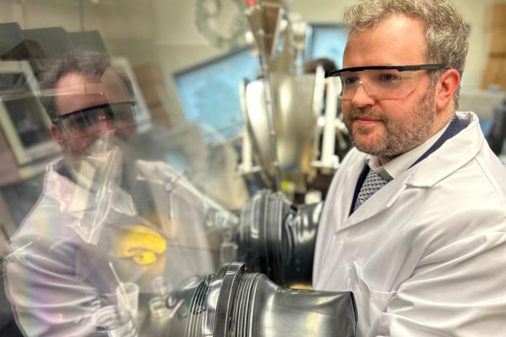
“Because there has never been the means to predict which materials will behave like this, and produce nanosheets with the properties we need to unlock various applications, only a handful of 2D materials have ever been processed into networks of printed 2D transistors,” said Tian Carey (pictured above), a newly appointed Royal Society–Research Ireland research assistant professor from Trinity College Dublin’s School of Physics and AMBER, the Research Ireland Centre for Advanced Materials and BioEngineering Research.
“Here, we’ve shown that we can unlock dozens of new 2D semiconductors. We’ve already fabricated state-of-the-art printed transistors with over ten new materials, unlocking new circuits for the first time. these include printed digital-to-analogue converters and BASK communication circuits, which are capable of encoding digital messages into high-frequency signals – the fundamental building blocks of modern computing.”
The key seemingly lies in ensuring 'in-plane stiffness; is higher than out-of-plane stiffness. This represents a measure of how resistant the material is to deformation when put under pressure from different perspectives (in-place being along the material; out-of-plane being perpendicular).
The research, led by Tian Carey, in collaboration with Jonathan Coleman and colleagues, now has a predictive framework pinpointing the stiffness thresholds required for successful exfoliation across many different materials.
Using this, they created high-aspect-ratio nanosheet inks and built working transistors and circuits from them, including the first printed DACs and communication circuits.
Carey added: “It’s very exciting to imagine a new wave of electronic innovations, all of which could be manufactured like printed newspapers one day in the future. In theory, this approach could yield abundant low-cost, flexible, and high-performance 2D electronics.”
“We now also understand from this work that each transistor's performance is limited by junctions between semiconductors rather than by defects within the semiconductors themselves, which is important in helping us direct future efforts. With this in mind, our next step will be to reduce the impact of these ‘flake-to-flake’ junctions to unlock the next big performance jump.”
Carey recently secured a Royal Society University Research Fellowship (URF) to build an independent research group in Trinity. He will now grow his team and lead a project that will develop printed electronics using 2D materials – specifically FETs and circuits.


