Low-pressure CVD of Ga₂O₃: Growth and beyond
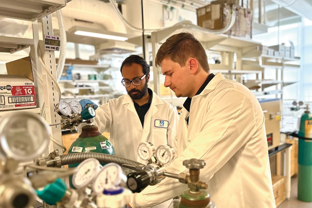
Advances in low-pressure CVD-based growth of Ga₂O₃ and its in-situ etching address two critical bottlenecks: high-quality, high-growth-rate films; and damage-free patternability.
BY ANHAR BHUIYAN FROM UNIVERSITY OF MASSACHUSETTS LOWELL
The world of power electronics is undergoing a radical transformation. Silicon’s long reign is nearing its limit and wide and ultra-wide bandgap semiconductors are taking centre stage, thanks to a number of strengths that include the capability to withstand high electric fields, switch at higher frequencies, and survive harsh environments.
At the forefront of this revolution is gallium oxide (β-Ga₂O₃), an emerging oxide semiconductor with an ultra-wide bandgap of 4.8 eV and a breakdown field exceeding 8 MV cm-1.
These are incredibly impressive numbers – they representing orders-of-magnitude advantages in power density and efficiency over not just legacy materials like silicon, but also the two leading wide bandgap champions, GaN and SiC.
Yet, for all its promise, Ga₂O₃ is still navigating the hurdles of real-world, scalable adoption. Its distinct material properties and complex crystallographic structure have introduced nuanced barriers that challenge conventional process strategies – especially when it comes to materials engineering at scale.
Figure 1. In the LPCVD system for Ga₂O₃ epitaxy, gallium pellets in the
source zone are heated and transported downstream by argon carrier gas.
In the growth zone, gallium adatoms react with oxygen at the heated
substrate surface to form crystalline β-Ga₂O₃ films. In the etch mode,
operated with only gallium and argon (without O₂ or SiCl₄), gallium
reacts with Ga₂O₃ to produce volatile Ga₂O, enabling smooth, damage-free
material removal.
Two of the most persistent obstacles that are stopping this oxide from fulfilling its promise are growth and patterning.
On the growth side, it’s a formidable challenge to produce thick epitaxial layers with a low background doping and smooth surface morphology, traits that are crucial for the construction of vertical power devices. A high mobility, a smooth surface and a high growth rate rarely go hand-in-hand, and managing impurity incorporation at scale is far from trivial.
The other obstacle occurs on the processing side – etching Ga₂O₃ into precise three-dimensional architectures is a major bottleneck. Etching, in essence, is the controlled removal material to allow flat layers to be shaped into vertical devices with trenches, mesas, and other critical three-dimensional structures. It is as important as growth itself, because without well-defined etch steps, it’s impossible to realise advanced device geometries.
Figure 2. Room-temperature Hall mobility versus carrier concentration
for β-Ga₂O₃. LPCVD-grown films show mobilities up to 162 cm² V-1 s-1
for homoepitaxy on (010) β-Ga₂O₃ native substrates, values comparable
to the best reports, but realised at higher growth rates. For
heteroepitaxial (2
Unfortunately, Ga₂O₃, with its anisotropic and complex monoclinic crystal structure, is notoriously difficult to etch with precision. Different crystal planes respond very differently to chemical or plasma environments, leading to rough sidewalls, undercutting, or material damage.
While conventional plasma-based dry etching can define vertical features, this comes with collateral damage – oxygen vacancies, deep trap states, and stoichiometric imbalances that degrade device reliability. And while wet etching is gentle, it has major limitations: it is typically isotropic, it lacks directional control, and it poses challenges for fabricating vertical, high-aspect-ratio structures.
The growth bottlenecks on one side and etching challenges on the other hinder the development of scalable Ga₂O₃ devices. This leaves those standing at this crossroads to ponder this question: Could there be a more unified approach to processing Ga₂O₃, one that addresses growth and patterning together?
Figure 3. Transport and doping characteristics of
LPCVD-grown silicon-doped β-Ga₂O₃.(a) and (b) Temperature-dependent Hall
measurements show peak mobilities of 843 cm² V-1 s-1 for heteroepitaxial (2
Our team at the University of Massachusetts Lowell has been considering this, and we think we have an answer, obtained by exploring an underutilised yet powerful technique – low-pressure CVD, or, for short, LPCVD.
This deposition technology has a number of strengths that are worthy of deeper investigation. Thanks to the reliance of LPCVD on an ultra-high-purity solid-source metallic gallium precursor, there’s a cleaner reaction environment than conventional metal-organic approaches, significantly reducing the risk of carbon, hydrogen or chlorine contamination and parasitic impurity incorporation – these are issues often observed in MOCVD and HVPE systems. Operating under high-temperature, low-pressure conditions, LPCVD supports rapid epitaxial growth and finely tuned surface kinetics, making it particularly well-suited for the deposition of thick, low-doped β-Ga₂O₃ layers with ultra-high purity.
What began as an exploration of growth efficiency soon revealed something more. As we pushed LPCVD to deliver high-purity, high-mobility β-Ga₂O₃ films, we realised the same environment could also be leveraged for etching. By shifting our conditions, we transition our process from deposition to the controlled removal of material, opening the door to a plasma-free, in-situ etching technique that carves smooth, anisotropic features into Ga₂O₃ with unprecedented control. In a single system – without plasma, without corrosive halides, and without organometallic precursors – we grow and pattern this oxide, effectively sculpting the foundations of power devices. This dual capability is not an incremental improvement – it’s a transformational step toward redefining how ultrawide-bandgap semiconductors like Ga₂O₃ can be processed at scale.
Figure 4. Secondary ion mass spectrometry profile of a silicon-doped LPCVD β-Ga₂O₃ (010) film. Data show uniform silicon incorporation across the epilayer, while background levels of carbon, hydrogen, and chlorine remain below detection limits, highlighting the high purity of LPCVD growth.
The growth bottleneck
High-quality drift layers are the bedrock of vertical Ga₂O₃ devices. But the path to growing them at scale has been littered with compromise. MOCVD, while widely adopted, involves metal-organic precursors that introduce carbon impurities with surface defects and cracks, particularly when cranking up the growth rate. The hallmark crystalline quality of this deposition technology is offset by sluggish growth rates and parasitic reactions that erode yield. HVPE, on the other hand, accelerates growth, but leaves behind rough surfaces that necessitate chemical-mechanical polishing. The other obvious contender, MBE, provides atomic precision and tight doping control, but is impractical for thick-layer growth, due to painfully slow deposition rates and high operating costs.
This is where LPCVD begins to shift the narrative.
Our team is using a home-built LPCVD reactor that’s fed with elemental gallium and oxygen precursors (see Figure 1). Ultra-high purity argon provides the carrier gas. Using this reactor, we observe a confluence of purity, growth rate, and control that is difficult to achieve in Ga₂O₃ epitaxy. Operating at 1000 °C and 1.5 Torr, with a carefully optimised source-to-substrate spacing for uniformity, we realise growth rates as high as 17 µm hr-1. These rates are an order of magnitude higher than typical MOCVD and MBE, and are on par with HVPE, but with smooth surfaces and ultra-clean material quality.
The electrical performance of these films breaks new ground. Our homoepitaxial (010) β-Ga₂O₃ films have room-temperature Hall mobilities of 162 cm² V-1 s-1 at a carrier concentration of 1.5 × 10¹⁷ cm-3 – these values are fully comparable with the best reported from state-of-the-art growth techniques, but obtained using far higher deposition rates (see Figure 2). Even more striking, our heteroepitaxial (2
Figure 5. The LPCVD system can provide in-situ etching of β-Ga₂O₃ via
the selective reaction of gallium adatoms with exposed β-Ga₂O₃ surfaces
to form the volatile Ga2O suboxide. This enables anisotropic, plasma-free etching through SiO2 mask-defined regions.
We enjoy great versatility when using a SiCl₄ gas precursor to provide silicon doping. Adjusting the flow rate tunes the carrier concentration across more than two orders of magnitude, from 1 × 10¹⁷ cm-3 to beyond 1 × 10¹⁹ cm-3, while preserving excellent crystal quality. Results from structural analysis are unambiguous: X-ray diffraction shows rocking curves as narrow as 63 arcsec, Raman confirms phase-pure β-Ga₂O₃ with no secondary phases, and atomic force microscopy scans offer evidence of atomically smooth surface morphologies.
But beyond numbers, what makes LPCVD truly powerful is how it handles purity. According to secondary ion mass spectrometry, our films have extremely low levels of carbon, hydrogen, and chlorine, well below the detection limits of this technique (see Figure 4). This strength is especially notable when comparing the purity of our films with those grown by trimethylgallium-based MOCVD processes, which struggle with residual carbon, even under aggressive purging. Note that the absence of carbon is not just a purity metric; it directly impacts compensation, carrier scattering, and long-term reliability.
Figure 6. Tilted field-emission scanning electron microscopy images of
etched trench arrays along different crystallographic orientations on
(010) β-Ga₂O₃, showing variations in fin width and sidewall morphology.
The polar plot of lateral etch rates at 1000 °C and 1050 °C highlights
strong anisotropy: the (100) orientation shows the most stable, vertical
sidewalls, while (101) exhibits the fastest lateral etching, consistent
with its higher surface energy and lower stability. For more details,
see Khan et al. Appl. Phys. Lett. 127 102105 (2025).
Taken together, our results highlight that LPCVD is more than just another growth method. It is a scalable, tuneable, and remarkably clean platform for producing high-quality thick β-Ga₂O₃ films.
But we soon discovered that’s only half the story. The real power of LPCVD lies in its duality: not just growing Ga₂O₃, but shaping it. Read on to discover of how LPCVD also provides plasma-free, orientation-selective etching.
Etching without scars
Etching β-Ga₂O₃ has long been one of its most persistent processing challenges. While plasma-based etching with BCl₃/Cl₂ produces vertical profiles, they tend to suffer from surface damage, oxygen vacancies, and trap states that degrade device performance through premature breakdown and higher leakage. Turning to wet etching avoids plasma-induced damage, but this technique is isotropic, slow, and lacks the control needed for vertical, high-aspect-ratio structures. There are other approaches, such as metal-assisted etching, but challenges remain, including relatively low etch rates and a reduced Schottky barrier, due to surface oxygen loss and reconstruction. Even emerging in-situ approaches based on MBE or MOCVD encounter challenges, with researchers grappling with gallium droplet formation and the need for additional cleaning/etching steps before regrowth.
These persistent hurdles raise an intriguing possibility: could Ga₂O₃ be etched in the same controlled, damage-free way that it is grown?
That’s what we set out to explore, using our LPCVD platform developed for Ga₂O₃ growth and pivoting it toward etching. To accomplish this switch, we introduce metallic gallium in the upstream zone, heating it in tandem with the substrate. These conditions cause a vapour-phase suboxide reaction to take place in situ, with gallium and Ga₂O₃ reacting to produce the volatile suboxide Ga₂O. Under a flow of argon, Ga₂O is swept away to leave etched features, crucially without the telltale scars of plasma damage (see Figure 5). There’s no ion bombardment and no reactive radicals. Just a thermodynamically driven surface reaction that respects the underlying crystal structure.
Our experiments have involved etching temperatures between 1000-1100 °C and pressures around 0.5-2.1 Torr. These conditions enable etch rates as high as 2.25 µm hr-1 – that’s orders of magnitude faster than a typical wet etch, and competitive with plasma-based dry etches, but without the collateral damage. This clean, controllable performance highlights the promise of our approach.
Figure 7. Quasi-vertical β-Ga₂O₃ Schottky barrier diodes fabricated
entirely within an LPCVD process flow on a sapphire substrate. (a)
Device schematic showing the epitaxial stack and contacts. (b) Forward
current-voltage characteristics show a low turn-on voltage of 1.22 V, a
differential on-resistance of 8.6 mΩ cm² and an ideality factor of 1.29,
reflecting solid diode performance. (c) Temperature-dependent
measurements up to 250 °C show stable forward conduction and
rectification ratios consistently above 10⁵. For more details, see Khan
et al. APL Electronic Devices 1 036125 (2025).
Beyond the high etch rate and clean surfaces, our gallium-assisted etching reveals a striking directional dependence. We discovered this by patterning radial trench arrays across (010) β-Ga₂O₃ substrates. Results reveal a stunning dependence on in-plane orientation. We found that trenches aligned with (100) orientations produce the cleanest, most vertical sidewalls – smooth, sharp, and nearly ideal. In contrast, those aligned along orientations such as (101) show lateral undercut, roughened sidewalls, and curvature at the trench bottom (see Figure 6).
We attribute this directional dependence to the surface energy and chemical stability of different Ga₂O₃ facets. The (100) plane, known for its low surface energy and high thermodynamic stability, offers minimal reactivity and promotes layer-by-layer removal. Meanwhile, planes like (101) possess higher surface energies, are less stable, and are thus more prone to lateral etching and microfacet formation.
Rotating trenches away from the (100) plane allowed us to observe a progressive evolution of sidewall morphology. This investigation determined that intermediate orientations produce stepped sidewalls, made up of competing crystal facets; and as the direction shifts further, one facet family begins to dominate, stabilising the etch profile along that orientation.
In other words, the anisotropy isn’t imposed by a plasma sheath or a lithography trick; it emerges naturally from the crystal structure. This self-selecting behaviour, a kind of thermodynamic ‘etch relaxation’, offers fresh insight into gallium-assisted Ga₂O₃ etching in LPCVD systems, and highlights a controllable, damage-free path for building vertical device structures.
The most exciting aspect is that this plasma-free process opens new doors to the monolithic integration of vertical 3D structures. There is the tantalising prospect of growing and etching Ga₂O₃ in the same chamber, and tuning anisotropy through the judicious selection of crystal orientation, temperature, carrier gas flow and source-to-substrate spacing. That level of control, realised without the usual damage, is what scalable Ga₂O₃ device manufacturing needs.
Sculpting devices
However, what good is a new processing technique if it can’t deliver real devices?
That’s the question we asked ourselves after validating LPCVD as a platform for high-purity growth and plasma-free etching. With those successes under our belt, it was time to move from concept to consequence. But could this dual-purpose platform do more than simply demonstrate elegant chemistry and impressive materials data? Could it, in fact, aid the fabrication of real, vertical Ga₂O₃ power devices, on affordable substrates, with minimal processing steps and zero exposure to plasma?
Our goal was ambitious: the fabrication of quasi-vertical β-Ga₂O₃ Schottky diodes, entirely within the confines of an LPCVD-based process flow, starting from film growth on sapphire and ending with in-situ mesa isolation via gallium-assisted etching. No ion bombardment. No dry etch residues. No need for damage control. Just epitaxy, etching, and forming electrodes.
We began by loading c-plane sapphire, a readily available and cost-effective substrate, into our LPCVD reactor. Using a 6° miscut, we realised step-flow growth of (2
Next came the etch. Using the same reactor, we introduced solid gallium upstream to perform in-situ mesa isolation at 1050 °C. This allowed the volatile suboxide Ga₂O reaction previously studied to serve a new role: carving out 3D device topographies. With a SiO₂ mask in place, we etched 3.6 mm-deep mesas.
Our next step involved fabrication of quasi-vertical Schottky barrier diodes, featuring Ni/Au Schottky contacts atop the etched mesa and Ti/Au cathodes contacting the recessed n+ layer. These devices delivered strong, clean forward characteristics. The turn-on voltage landed at 1.22 V, the ideality factor hovered at 1.29, and the Schottky barrier height was 0.83 eV. Importantly, these diodes handled forward current densities up to 252 A cm-2 and exhibited a differential specific on-resistance of just 8.6 mΩ cm².
And they held up under stress. When ramping from room temperature to 250 °C they didn’t flinch. The ideality factor rose only slightly, and the reverse leakage remained modest, climbing from 5 µA cm-2 at 25 °C to just 170 µA cm-2 at 250 °C. Even at the highest temperatures tested, the rectification ratio remained above 10⁵.
Under reverse bias, our devices exhibit blocking voltages of up to 100 V, corresponding to electric fields approaching 2 MV cm-1. While these values are still below the theoretical potential of Ga₂O₃, they are primarily limited by the drift layer design, and specifically, the relatively high doping in the drift layer. According to TCAD simulations, electric field crowding near the anode perimeter also plays a role in early breakdown. Much higher blocking voltages can be readily achieved with optimised edge termination, thicker drift layers, lower doping profiles and the introduction of a high-permittivity dielectric.
Even so, our results clearly validate the LPCVD processing platform: within a single system we demonstrate high-quality growth, damage-free etching, and the fabrication of β-Ga₂O₃ Schottky diodes on low-cost sapphire – all without plasma exposure or post-etch recovery.
From process to platform
What makes LPCVD uniquely powerful is not just its ability to grow or etch, but to unify both in a single platform. Instead of relying on separate tools for deposition, doping, and patterning, one can undertaken growth and orientation-selective etching in a continuous flow with LPCVD, without breaking vacuum. This brings clear advantages in yield, cost, and scalability.
Our approach is intrinsically modular and scalable. By using solid-source metallic gallium, many impurity risks inherent in metal-organic chemistries are eliminated. The absence of a plasma ensures preservation of surface integrity, critical for Schottky interfaces, gate dielectrics, and regrown junctions. And as devices increase in complexity – through the introduction of deep trenches, vertical fins, or dielectric caps – the value of our low-damage, chemically selective etch-and-regrowth strategy will become even more pronounced.
As the power device community pushes toward deeper verticality, higher voltages, and more thermally demanding systems, platforms like LPCVD – modular, directional, and clean – will not just be useful, but essential. By uniting growth and etching in one coherent process, LPCVD will transform Ga₂O₃ fabrication from a collection of disconnected steps into a scalable platform – and one that’s capable of shaping the next generation of ultrawide-bandgap power electronics.
We gratefully acknowledge funding support from National Science Foundation (ECCS Awards 2501623 and 2532898) for this work.


