
PCSEL: Progressing the PCSEL towards high-volume production
By developing and refining the PCSEL, manufacturers of optoelectronic device are laying the foundations for the commercial success of this very promising class of laser.
BY RICHARD STEVENSON, EDITOR, CS MAGAZINE
Taking a device from its inception to lucrative, high-volume production is a lengthy, complex journey. Following the eureka moment that spawns a promising idea for a new class of device, there’s the fabrication of the first chip and then its development, demanding many years of funding, often secured by identifying a potentially ‘killer’ application. Design and processing must then improve, so that this device satisfies a long list of requirements, including those related to performance, yield, cost and reliability, prior to the commercial launch of a competitive product that will net significant sales. That last step is particularly tricky to navigate if the fledgling device will only succeed in the marketplace by displacing an incumbent, as then it’s critical that the new contender outperforms its rival by significant margins to win over the wavering minds of system engineers that are responsible for placing orders.
Against this backdrop, how much progress has been made by the PCSEL, the surface-emitting single-mode laser with a photonic structure that’s renowned for its exceptional beam profile, incredibly narrow divergence, and a power that scales with the size of the emitting region?

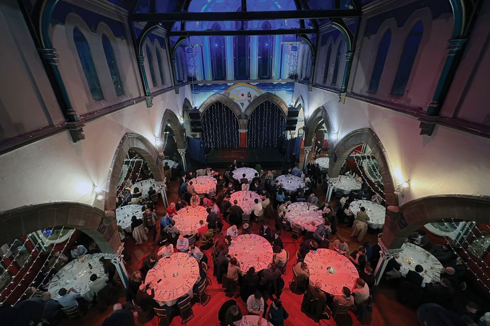
On the first evening of the conference, delegates were offered a guided tour of Clydeside Distillery.
While it’s never possible to offer a definitive answer to this crucial question, those attending the recent second International Workshop on the PCSEL could offer an informative, well-considered answer. At that gathering, held on 10-12 November in Glasgow, UK – and co-located with the 14th International Symposium on Photonic and Electromagnetic Crystal Structures – a number of companies and universities detailed advances in the performance of the PCSEL. And during networking events, including a delightful visit to a local distillery, a number of low-profile delegates disclosed that they were also pursuing the development this promising surface-emitting laser, either at a company looking to diversify its laser portfolio or a new start-up formed to champion this device. So, what’s clear is that there’s tremendous momentum behind the PCSEL, with much effort directed at preparing the ground for commercial success.
Laying much of the foundation for progress to date is Susumu Noda, the leader of PCSEL development at Kyoto University, and a co-author of the first ever paper outlining this device, published back in 1999 in Applied Physics Letters. Since that ground-breaking conception, Noda’s group has made a great deal of progress on many fronts, including the production of numerous devices, featuring higher powers and an expansion of material systems and spectral ranges.
Noda delivered the keynote session at the joint conference, with a presentation describing many potential applications for the PCSEL. They include using this device as the optical source for lidar employed in automobiles, farm machinery and robots; the deployment of PCSELs in material processing; and using this source for free-space communication, both underwater and over vast distances in space. In fact, there are so many applications where the PCSEL could serve that this situation may be viewed as an embarrassment of riches – with such a vast number of opportunities, it can be a challenge to know quite where to focus.
As one would expect in a keynote presentation, Noda covered a great deal of ground, highlighting key milestones from more than two decades of trailblazing research. While much of this would be familiar to many in the audience, the latest results, yet to be published, would be new to them. Building on powerful sources with an emission diameter of 3 mm, Noda and co-workers have just introduced variants with a diameter of 10 mm, emitting at around 940 nm. Initially, these sources produced more than 500 W of optical power when driven with pulses of 1000 A, and very recently continuous-wave outputs of 500-1000 W have been developed, with the PCSEL’s thermal management benefitting from its bonding to a sub-mount.
Today, the most efficient PCSELs have a wall-plug efficiency of around 25-30 percent. Noda suggested that far higher values, potentially up to 60 percent, might be realised by turning to multi-junction PCSELs.
Offering a tantalizing glimpse into the future, the PCSEL pioneer claimed that it may be possible to produce 15-20 kW devices with an emission diameter of 3 cm. Such sources would be a very attractive alternative to today’s CO2 lasers, which are bulky – typical dimensions are around 1.5 by 0.4 m by 0.5 m – and have an efficiency of about 10 percent.

Sumitomo Electric Industries has been developing InP PCSELs emitting
at 1.3 µm and 1.55 µm. (a) Schematic of these InP-based PCSELs. (b)
Light-current-voltage characteristics with far-field pattern (inset) and
(c) lasing spectra under continuous-wave operation.
A key member in Noda’s group, Takuya Inoue, focused on one of the applications mentioned in the keynote address, giving a presentation on the dynamic control of PCSELs for satellite communication. Inoue explained that satellite communication involves transmission over distances of more than 1000 km at data rates between 1 Gbit s-1 and 100 Gbit s-1. As only a fraction of the light leaving the transmitter will hit the detector, due to beam divergence, the source must produce an optical power of at least 1 W.
Outlining the requirements for the transmitter, Inoue remarked that “the size, weight and power must be as small as possible”. But these are not the attributes of a conventional transmitter, which incorporates an erbium-doped fibre amplifier that’s large and heavy. This transmitter also features a number of components, hindering reliability.
PCSELs have much promise for this application, thanks to their high power and incredibly narrow beam divergence. But what modulation speeds are possible?
Inoue and colleagues have been investigating this matter for a few years, with initial efforts determining watt-class operation with a direct bandwidth of more than 3 GHz. Turning to quadrature amplitude modulation has enabled transmission of 256 QAM signals at 2 Gbaud.
More recently, this team has investigated coherent free-space optical communication, realised with two-section PCSELs featuring a pair of photonic crystals with slightly different lattice constants in their gain sections. By injecting an anti-phase modulation current with the same bias current in both sections, the team have generated watt-class frequency-modulated signals with supressed amplitude modulation. This success provided the foundation for employing this PCSEL as a coherent free-space optical transmitter delivering Gbit s-1 signal transmission, even when laser power is attenuated by 80 dB. Success with such a degree of attenuation, corresponding to the link loss in satellite communication, allows Inoue to claim that the team’s directly modulated PCSELs have the potential to provide compact free-space optical transmitters for tomorrow’s satellite communication systems.
As well as running the world’s leading group on PCSEL development, Noda has inspired and supported a number of Japanese optoelectronic manufacturers in their development of this device. They include Hamamatsu Photonics, which launched the first commercial PCSEL in 2017 (a data sheet for this product, the L13395-04, can be found on the internet, but there is no price, suggesting it’s been discontinued).
Hamamatsu is continuing to develop its PCSELs, targeting applications requiring a patterned light source. During development of its lasers, one of the issues that’s been addressed is what’s described as ‘mesh noise’ – this arises from an anti-crossing of photonic bands between the fundamental mode and higher modes in the layer direction.
At the PCSEL workshop, company spokesman Yoshitaka Kuorsaka told delegates that these modes have now been eliminated. Details surrounding the solution were scant, but involved changes to the epitaxial structure. Another issue that’s been addressed is zero-order noise, removed by modifying the photonic crystal structure to introduce an additional phase.
Recent efforts by Kurosaka and co-workers have focused on a structure with two embedded regions in the same square lattice. The team have produced horizontal stripe patterns with a phase difference of 90 ° that have a stripe intensity ratio for each pattern region that changes continuously when the beams are superimposed. Based on this demonstration, Kurosaka claims that this work paves the way to a dynamically changeable light pattern consisting of multiple channels.
In related work, Kurosaka’s colleague Kazuyoshi Hirose detailed micro-pattern projection from a PCSEL-based on-chip pattern generator. These projections could be deployed for 3D profilometry – that’s the measurement of surface profiles – with high-quality patterns needed for practical application.
InP PCSELs
Another Japanese optoelectronics powerhouse that is partnering with Noda’s team for PCSEL development is Sumitomo Electric Industries. This firm is directing efforts at improving the performance of InP PCSELs emitting at 1.3 µm and 1.55 µm, viewing such devices as promising candidates for sensing, free-space communication and sources for optical communication networks.
The power of Sumitomo’s PCSELs has increased significantly over the last few years. Back in 2022, designs featuring a double-lattice produced an optical output of 200 mW. The introduction of a metal mirror the following year doubled output, and the latest PCSELs are emitting 700 mW, thanks to the introduction of an in-plane heterostructure.
Sumitomo spokesman Yuhki Itoh told delegates that the team began by switching from a single-lattice to a double-lattice to increase vertical radiation and hit 200 mW. This refinement produced a 25-fold hike in slope efficiency.
Introducing a metal mirror provided the next jump in output power, with this move enhancing carrier injection and reducing emission in unwanted directions. Thanks to these benefits, InP PCSELs emitting at around 1330 nm produce: a slope efficiency of 0.4 W A-1; output powers of more than 400 mW and 150 mW at 25 °C and 70°C, respectively; a wall-plug efficiency of more than 24 percent at 25 °C; and a side-mode suppression ratio exceeding 70 dB. Variants with the same design emitting at 1.5 µm produce a continuous-wave output of 300 mW at 25 °C, and a peak power of 32 W when driven with short pulses.
To address limitations associated with self-heating that led to the leaking of light, Itoh and co-workers have recently introduce an in-plane heterostructure. This refinement is accomplished by reducing the size of the air holes near the device periphery, a change that leads to a lowering of the photonic band-edge frequency and ultimately an enhanced in-plane optical confinement. With this modification, output power climbs to 700 mW, and wall-plug efficiency is 27 percent at 25 °C.
Itoh and co-workers have also investigated the reliability of their PCSELs. Results are encouraging, with no degradation observed when driving these devices for 2,500 hours at 105 °C.
Benchmarking these PCSELs against high-power DFB lasers also leads to promising findings, including a superior wall-plug efficiency, a higher side-mode suppression ratio and a much narrower beam divergence.
Into the blue
Most of the development of the PCSEL has involved GaAs and InP material systems. But to reach shorter wavelengths, these emitters must be formed with the GaN-based material system.
In Japan, much effort has been devoted to the development of surface-emitting lasers based on GaN and its alloys. More than a decade ago, Nichia made a number of early breakthroughs in GaN VCSEL performance, including the first device producing more than a milliwatt. And more recently, other Japanese leaders in optoelectronics have grabbed the headlines, with impressive output powers of 15.4 mW and 22.2 mW, announced at Photonics West 2019 by Sony and Stanley Electric, respectively. Later that year, Stanley followed this up with a paper in Applied Physics Express, detailing a Watt-class blue-emitting array of 16 by 16 VCSELs.
Given how hard it is to make progress with GaN-based VCSELs, mainly due to issues associated with producing the mirrors – there’s no ideal lattice-matched pairing with a high refractive index contrast and good electrical conductivity – it’s not that surprising that Stanley Electric has also started to develop GaN-based PCSELs. Efforts on this front were presented in Glasgow by Mei Emoto, who described the progress of a collaboration between researchers at Stanley Electric and Kyoto University.
Emoto began by putting recent efforts in context, explaining that Noda’s group produced the first ever GaN-based PCSEL, reporting that success in 2008. That breakthrough emitter, featuring a triangular lattice and air holes, had a very high threshold of around 70 kA cm-2. Weaknesses of that pioneering PCSEL included insufficient resonance, a large scattering loss and a low slope efficiency.
To produce a higher-performance device, Emoto and co-workers switched to a square lattice to enhance optical confinement, optimised the size of the resonator, and developed a SiO2-free fabrication method. In addition, they have worked to improve crystal quality, aided by the use of GaN substrates. With these changes, PCSELs with a period for the holes of around 200 nm have a threshold current of around 2.6 kA cm-2.
Further improvements have resulted from the introduction of a double lattice that enhances vertical emission and in-plane resonance. With this refinement the team produced a single-mode PCSEL with an output of 1 W, emitting at 431 nm from a circular region with a diameter of 300 µm.
Even higher powers have come from an increase in the emission area to a diameter of 500 µm. With this change, output power exceeds 2 W, realised with a slope efficiency of 0.5 W A-1.
Emoto revealed that one of the issues with that generation of PCSELs is that as the current through the device is cranked up, there is a slight widening of the beam divergence angle. To address this, the team modified the design of its high-power PCSELs, increasing destructive interference to cut off the higher modes. With this optimisation, PCSELs have a stable fundamental mode, a threshold current of around just 1.8 kA cm-2, a slope efficiency of 0.6 W A-1, and an output power of more than 2 W.
The most recent results may be even more impressive. While Emoto failed to divulge many details, emitting area has increased to a diameter of 1 mm, and the divergence angle is just 0.5 °.
Emoto concluded his talk by showing how the team’s PCSELs can be used for underwater lidar, operating in systems with a 10 m range, and revealing that they have just started to collaborate with Nichia on the development of these devices.
UK efforts
Within the UK, the host nation for the workshop, there are efforts at developing PCSELs. This includes engineers at Huawei investigating these devices at the legendary facility in Ipswich, previously owned by BT and Corning, and recently renamed as the Bragg Research Centre. Here, efforts are focused on InP PCSELs, primarily for optical communication.
Speaking on behalf of PCSEL efforts at Huawei, Samir Rihani argued that the communication sector has fuelled laser innovation for many decades, driving the development of distributed Bragg reflector lasers in the 1970s; and in the data era that started in the 1990s, the first killer application of the VCSEL. And now with the growth of machine learning and AI, applications that demand massive parallel data transfer, there’s an opportunity for a compact, high-power laser, ideally operating at multi-wavelengths – and these requirements could be fulfilled by the PCSEL.
Working towards this, Rihani and co-workers have developed an InP-based multi-wavelength PCSEL with four channels, operating at around 1330 nm. This source has a wall-plug efficiency of 16 percent, and a power-per-channel of 45 mW at a drive current of 250 mA channel. Operating at up to 85°C, the slope efficiency for this PCSEL is 0.24 W A-1.
According to Rihani, the team’s quad-PCSEL has good channel uniformity, with a channel flatness of less than 1 dB, meeting the requirement for a multi-wavelength light source. The researchers have demonstrated a channel spacing of 0.6 nm, laying the foundations for a 32-channel PCSEL.
Rihani’s colleague, David Moodie, outlined the development of a 1550 nm PCSEL with a hetero-lattice design, created in collaboration with researchers at the University of Nottingham. Moodie explained that the motivation behind this design is an increase wall-plug efficiency, realised by reducing in-plane loss.
In addition, Moodie and co-workers have tried to optimise the round-trip phase from the photonic crystal to the p-metal reflector. This investigation involved etching of the p-type InP by either 0 nm, 61 nm, 122 nm or 183 nm, prior to addition of p-contact layers.
To produce the hetero-lattice PCSEL, the team defined an inner lattice, occupying a 200 µm square area, and featuring a double-lattice design – one lattice is shifted vertically and horizontally by a quarter of the 477 nm pitch. In addition to this inner lattice that has a 12.6 percent fill factor, the engineers formed a second photonic crystal that occupied the remainder of the 300 µm by 300 µm area. For this photonic crystal, there’s a 15.5 percent fill factor, and circular holes with half the pitch of the inner fill factor.
According to Moodie, the best results came from PCSELs with no p-type etching. For these devices, the introduction of the hetero-lattice increased the slope efficiency by 34 percent, boosted the output power, improved linearity, and ensured that the laser continued to operate in single-mode at higher current densities. Hetero-lattice PCSELs produced single-mode lasing at up to 85 °C.
Measurements of these PCSELs recorded powers of 249 mW and 145 mW at 25°C and 55°C. Driven at 2.5 A, side-mode suppression ratio exceeded 65 dB at both these temperatures.
Moodie told the delegates in Glasgow that the team are also developing 1300 nm PCSELs, and getting “good” results.
Given the location of the workshop – it’s in the backyard of Vector Photonics, a pioneer of the PCSEL – an absence of any presentations from the start-up, including any posters, will have raised a few eyebrows, particularly as this company initially had a very public profile. Over its first five years it has undergone major changes, including the departing of two of the four co-founders, including the CEO, as well as a Sales and Marketing Director. While such an upheaval might suggest a company in turmoil, it would be wrong to read too much into these developments. Vector is taking on new staff, with some at the conference, and it is making progress. As efforts are commercially sensitive, this restricts opportunities to details successes, accounting for the restricted engagement in Glasgow.
State of play
The second International Workshop on the PCSEL concluded with a discussion between all delegates on potential stumbling blocks to the commercial success of this laser. There are no major concerns related to the manufacturability of this device, and when its production moves to larger substrates, this will enable the use of better tools that increase yield and performance.
Proving reliability may not been a significant stumbling block either. Initial results are encouraging. As well as findings by Sumitomo, already described in this conference report, investigations by Changchun Institute of Optics, Fine Mechanics and Physics are encouraging – they determined an extrapolated lifetime of just over 8,000 hours, based on pulsed operation at 25 °C (10 kHz, 4.75 ns); and an accelerated aging lifetime test at 85 °C using the same pulse conditions led to no obvious degradation over 240 hours, indicating a life span of 3,288 hours. However, there is no standard for lifetime testing, an issue that may hamper commercial success.
In many applications, the wall-plug efficiency is a critical metric. For PCSELs, the best efforts have been around 30 percent. In contrast, for GaAs-based laser diodes, this figure is above 70 percent. For that class of laser, efficiencies increased about 20 years ago, spurred on by a DARPA-funded programme known as SHEDS – super high-efficiency diode sources. This effort, which included identification and quantification of loss mechanisms, provided funding for US companies to increase efficiencies from around 50 percent to 65 percent within 18 months. If successful, further funding followed, for an 80 percent target. Maybe a similar focus on the origins of losses in PCSELs, and addressing them, could spur improvements in this area? Offering hope, Noda revealed that his team have recently delivered a substantial hike in efficiency, with results soon to be published.
The biggest issue facing the PCSEL is what will be its ‘killer’ application. But rather than identifying this, maybe there’s a need to walk before running – that is, find a market that will allow a ramp to relatively modest volumes, providing a platform to target bigger successes.
While a lack of answer to this key question may seem deflating, it’s worth noting that many in the audience are industrial researchers. If they have identified a potential market for the PCSEL, why would they share this crucial advance with their competitors?
So, it’s possible that when delegates reconvene in 2027 for the third International Workshop on the PCSEL, at least one of the commercial pioneers will be starting to enjoy commercial success with this most promising class of laser, which continues to advance on many fronts.


