Displacing GaAs in handsets by 2030
Finwave’s roadmap for the commercialisation of its GaN-on-silicon technology begins with switches and amplifiers for infrastructure, will continue with penetration into the handset.
BY RICHARD STEVENSON, EDITOR, CS MAGAZINE
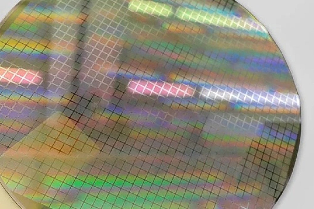
Over the last 30 years, opportunities for GaAs microelectronics have narrowed. In the final decade of the twentieth century, digital GaAs served in the infrastructure of optical networks, driving a number of components, including lasers, transimpedance amplifiers and multiplexers. After silicon and SiGe components took over, following the bursting of the dot-com bubble, the RF domain has accounted for all sales of GaAs transistors. While some revenue has come from defence and network infrastructure, the handset is responsible for the lion’s share. Initially, GaAs pHEMTs provided the switching function, before they were displaced by silicon-on-insulator technologies, leaving the main role for GaAs as power amplification. But this is now under threat, with US firm Finwave predicting that GaN will be taking on this task in handsets by the end of this decade, while enjoying additional sales from its deployment as a switch and power amplifier in infrastructure and aerospace and defence applications.
According to the CEO of Finwave, Pierre-Yves Lesaicherre, the reason why GaN will trump GaAs in the handset PA is that the incumbent is running out of steam above 6 GHz. “The power efficiency is just too low,” claims Lesaicherre, pointing out that Finwave’s enhancement-mode MISFET technology, which can run off a 5 volt supply, offers a high power-added efficiency from 6 GHz up to 40 GHz. These strengths, combined with the capability to deliver a high power-density, ensure that the GaN MISFET a compelling candidate for amplification for WiFi 7, for the FR3 band that’s used for 5G communication, and for bands that will be used for 6G communication.
Displacing GaAs PAs is a long-term goal for Finwave, which has made progress on many fronts since Lesaicherre took charge in summer 2023.
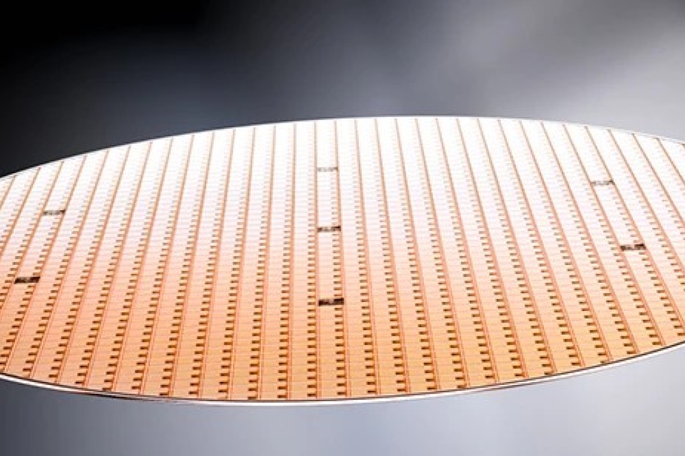
A spin-out of MIT, Finwave still has roots in the locality. Roughly half of the 23-strong team are located in Waltham, near Boston, working on processes and device architectures associated with the company’s proprietary GaN-on-silicon technology.
The remainder, responsible for product design, product engineering test and quality, and supply chains, are located in San Diego, California. “We have moved to a larger office in the Sorrento Valley next to pSemi and Qualcomm,” says Lesaicherre.
Also helping to lay foundations for further success are the hiring of a few additional RF designers, the appointment of a VP of Marketing and a chief financial officer, and the establishing of partners for device production.
“In August '24, we signed a technology licencing and transfer agreement with Global Foundries to transfer our low-voltage E-Mode MISHEMT RF GaN-on-silicon technology for handset applications,” says Lesaicherre. “This technology is unique, and it's being transferred to an 8-inch fab in Burlington, Vermont.”
The second key partnership that’s been cemented in the last few months is with a leading foundry in Taiwan, which has started producing Finwave’s RF switches and high-power amplifiers for communication and infrastructure applications.
To produce packaged devices, Finwave has another partner, Unisem, in Malaysia. This provider of back-end services is described by Lesaicherre as a leading test and assembly house for RF semiconductors.
Recently, Finwave’s supply chain has been refined through its introduction of a product life management system and a quality management system. And a sales ramp over the coming years will be supported by a distribution agreement with a leading RF distributor, the details of which should emerge in the next few weeks.
Finwave’s product roadmap
Finwave’s goals for the first half of this year include process and product qualification of its first RF switches in quarter one, 2025, followed by a ramp in sales of the first three RF switches in the subsequent quarter.
“The products are 10-watt, a 20-watt, and a 40-watt RF switches that operate from a few megahertz to 13 gigahertz,” reveals Lesaicherre, who argues that these devices offer a unique and compelling combination of assets. They have a capacity to handle high powers and frequencies, and they have very fast switching and settling times –just hundreds of nanoseconds.
Lesaicherre says that one of the one weakness of switches based on silicon-on-insulator (SOI) technology is their limited power handling, as they struggle with signals above 10 watts.
“We see our product more of an extension of the RF SOI switch, rather than a direct competitor,” remarks Lesaicherre. “Now, we're competing with GaN-on-silicon carbide switches, but at a much lower production cost, which gives us a major pricing advantage.”
Finwave’s switch portfolio will expand this year, due to the introduction of many more products. Improved performance is also in the pipeline, with the company working on second-generation technology.
Switches produced by this fabless firm could serve in a number of applications in both defence and infrastructure sectors. Many opportunities exist, including those in radar, miliary radio systems and base stations.
As well as growing its switch portfolio, Finwave is focusing on the commercialisation of high-power amplifiers, operating at typically between 15 volts and 28 volts, for communication infrastructure.
“The main competition here is also GaN-on-silicon carbide,” claims Lesaicherre. “Again, we have a major cost advantage, and also the ability to scale to eight-inch wafers, and possibly 12-inch wafers in the future.”
An additional, exciting opportunity for Finwave is the possibility to integrate the PA, the low-noise amplifier and the switch on a single GaN-on-silicon chip. According to Lesaicherre, such a technology promises significant cost and integration advantages over today’s RF front-ends, which combine multiple chips, manufactured using different material systems. “We think that's a key differentiator for telecom infrastructure.”
For the third opportunity Finwave has identified – displacing the GaAs PA in the handset – the higher performance that GaN-on-silicon provides and the possibility to produce a single chip that incorporates a PA, a low-noise amplifier and a switch could fuel the growth of GaN-on-silicon technology.

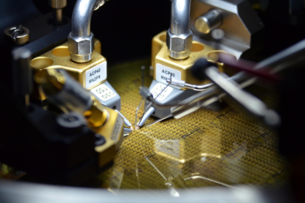
Finwave’s RF Switches mounted on an evaluation board
A shift in focus
When Finwave spun-out of the labs at MIT, initially under the moniker Cambridge Electronics, it attracted much attention for its finFET technology. While this is not being used in its emerging switch and power amplifier products, all based on planar architectures, it has not discarded this novel approach to transistor design. “We've also demonstrated that with a 3-D finFET architecture we can improve linearity for D-mode power amplifiers for infrastructure, but we are not yet producing these,” reveals Lesaicherre.
Another shift in focus over the last few years has been a move away from pursuing success in the power electronics sector to concentrating on opportunities in the RF domain.
“We had some interesting developments on low-voltage and medium-voltage GaN technology, so we believe our technology is capable of addressing this market, but our current focus is solely on RF applications,” insists Lesaicherre. “We've got a lot on our plate with the development of a full range of RF switches and power amplifiers.”
Focusing on RF applications, where there are far fewer competitors than there are for GaN power electronics, promises to generate significant sales. According to Lesaicherre, the total addressable market in the 2028 to 2030 timeframe is a few billion dollars per annum for amplifiers in cellular infrastructure, and $4-5 billion for amplifiers in handsets. Given these figures, there’s great potential for substantial growth for Finwave throughout this decade and beyond.