300 mm SiC: A format for when?
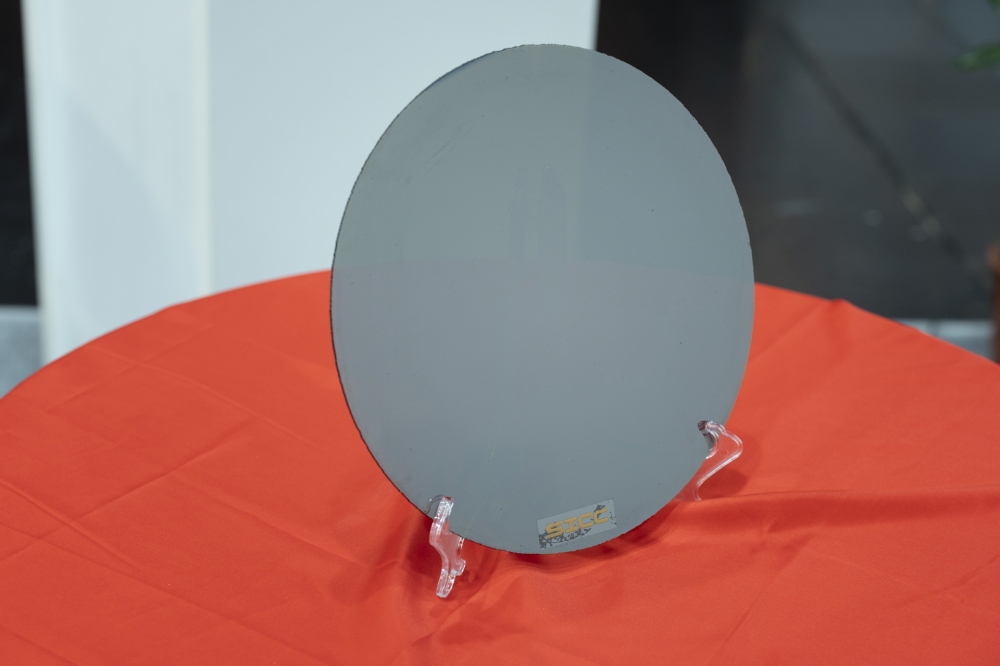
Is the unveiling of a 300 mm SiC substrate by SICC going to drive a
relatively rapid shift to high-volume production with this format?
BY RICHARD STEVENSON, EDITOR, CS MAGAZINE
Those in our industry will probably remember the recent Electronica for the unveiling of the world’s first 300 mm SiC substrate. This breakthrough, showcased to the world in mid-November from Munich, Germany, is undoubtedly a great demonstration of technical prowess. But is it going to have an impact in an industry that is only just starting to make the transition from 150 mm to 200 mm SiC lines?
Some may argue that this triumph, realised by one of the world’s biggest manufacturers of SiC, SICC of Jinan, China, is of little relevance in the near term, but the trailblazer sees the situation differently.
Speaking of its behalf, Chairman Yanming Zong told Compound Semiconductor that one of the purposes behind this demonstration is the promotion of industrialisation of 300 mm SiC. While the rate of technical progress and the level of demand for this new format will influence the precise timing of SICC’s commercialisation of 300 mm n-type SiC substrates, the anticipation is that small production volumes will begin in 2027.
At this stage, it’s unclear which chipmakers will be keen to buy this new format. However, Zong believes that some of the leading makers of SiC devices may be willing to invest in upgrading their lines to trim costs, and he points out that some start-ups may see the benefit of beginning with larger wafers.
For all those making SiC devices, weighing on production costs is the slow growth rate of the boules, which are sliced to form substrates.
“We want to continuously reduce the cost of material per unit area by expanding the substrate size,” remarks Zong, who hopes that one of the consequences of introducing larger wafers will be an increase in the bang-per-buck of SiC devices.
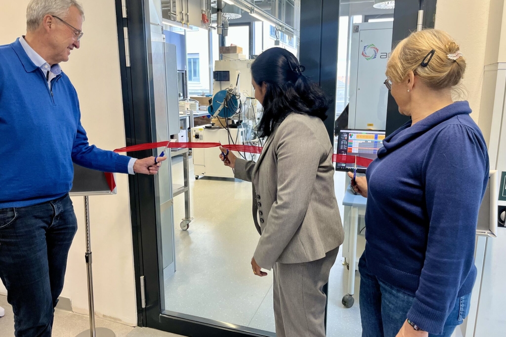
SICC unveiled its record-breaking 300 mm SiC n-type substrate at
Electronica, held in Munich, Germany, in mid-November. On the left is
the company’s Chairman Yanming Zong, and on the right its CTO, Chao Gao.
Swift scaling
Founded in 2010, SICC, which focuses on the R&D, production and sales of SiC substrate material, used equipment designed and installed by its R&D team to produce the record-breaking substrates. This multicultural, highly qualified team took just 18 months to enlarge its n-type boules from 200 mm to 300 mm.
The ground-breaking enlarged boule, produced using the same axial growth rate employed for manufacturing of 200 mm material, has a thickness of around 20 mm. From this ingot, it is possible to slice around 25 to 35 wafers with a thickness of 500 µm. And as the team refines its process, it will be possible to produce thicker boules that yield more wafers.
Historically, SiC substrates have been plagued with a variety of imperfections that degrade and even kill devices. However, those issues have now been addressed by many companies, and as the process that’s used to fabricate the 300 mm substrate is the same as that used to produce smaller wafers, there is no major barrier to realising state-of-the-art quality with the larger format.
Encouragingly, one of the critical defects, the micropipe, is not a significant issue in SICC’s n-type 300 mm substrate. With further development, micropipe density is forecast to fall to below 0.2 cm-2, which is a degree of prevalence found in the company’s 200 mm n-type SiC.
Of more concern are basal plane dislocations. However, while this class of defect needs to be reduced, the company is confident it can replicate the density found on its 200 mm n-type substrates.
Efforts will not have to be directed at improving surface roughness. SICC’s 300 mm substrate has a roughness of just 0.2 nm, a figure comparable to that for the company’s 200 mm wafers.
One of the next steps on the road to commercialisation is the verification of the quality of the epilayers produced on 300 mm substrates. Today, none of the suppliers of MOCVD reactors have tools designed to accommodate this size. However, Zong argues that they will have anticipated the unveiling of this format, and he does not expect tool availability to hold back progress.
The n-type 300 mm format that SICC is pioneering is suitable for producing power devices that operate at high voltages and high frequencies and are deployed in inverters and electric vehicles.
As well as being the world’s second biggest producer of n-type SiC, SICC has other SiC-related products in its portfolio, including a heat dissipation SiC bare product that is said to combine exceptional thermal stability with ultra-high thermal conductivity.
For the last five years SICC has been the third largest producer of semi-insulating SiC, a popular platform for RF products. It also offers p-type SiC, the ideal platform for producing bipolar SiC IGBTs, which are attractive candidates for deployment in high-power electronic systems, such as smart grids – they require devices than can handle 10 kV or more.
A novel growth process


