
The tantalising promise of wider bandgaps
Producing power devices with ever wider bandgaps is far from easy, but realising success slashes on-resistance while boosting blocking capability
One of the primary purposes of CS International is to provide a detailed overview of the latest trends with our industry. To fulfil this goal, the key themes of this conference have evolved over the last 15 years. While progress in GaAs RF electronics played an important role in the first few meetings, this has subsequently taken a back seat, with CS International now focusing on optoelectronics and power electronics, with the latter accounting for the lion’s share of the 40 or so presentations.
Today, SiC accounts for the majority of the revenue generated by compound semiconductor power electronics, and sales are forecast to continue to climb, as many of the leading suppliers expand their production capacities, enhance their portfolios, and ship more products for deployment in electric vehicles.
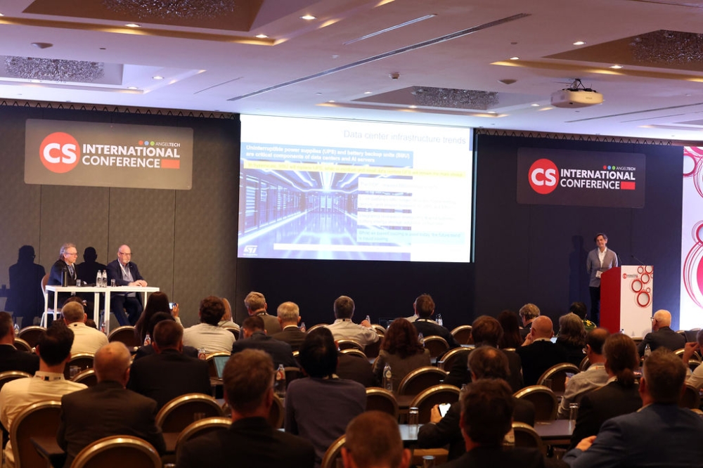
At this year’s CS International – held at the Sheraton Hotel, Brussels, from 8-9 April – two leading chipmakers, Navitas and Infineon, detailed the strengths of their approaches in a session entitled Optimising opportunities for SiC success.
Speaking on behalf of Navitas, Senior Director for Product Management and Marketing for SiC and GaN, Llewellyn Vaughan-Edmunds, discussed the company’s novel trench-assisted planar technology for SiC MOSFETs.
Vaughan-Edmunds argued that while the traditional planar architecture offers repeatable high-yield, low-cost manufacture, and has a high level of reliability that benefits from a rugged gate oxide, which ensures a stable threshold voltage, these strengths come at the expense of slow switching and high values for the drain-source on-resistance, both as a function of area and as a change in temperature.
According to Vaughan-Edmunds, the SiC trench MOSFET also has some significant weaknesses. While this design addresses the shortcomings of the traditional MOSFET, this class of transistor suffers from an inconsistent trench etch that hampers yield and leads to higher production costs. What’s more, reliability is impaired by failures from the non-uniform gate oxide, and the device is held back by a lower short-circuit capability.

The Navitas trench-assisted planar MOSFETs
Offering the best of both worlds, says Vaughan-Edmunds, is the trench-assisted planar SiC MOSFET. It is claimed to combine the manufacturing merits of the planar MOSFET with the performance of its trench-based cousin, while excelling in reliability – this design has excellent avalanche capability, a long short-circuit withstand time, and features a rugged gate oxide that ensures a stable threshold voltage.
To benchmark the performance of Navitas’ trench-assisted planar MOSFETs, Vaughan-Edmunds presented a plot of the key figure of merit – the product of the drain-source on-resistance and area – for currents up to 100 A. The Navitas device delivers the most impressive performance, with the next-best values coming from the planar devices produced by Toshiba and General Electric.
Vaughan-Edmunds also discussed the pros and cons of various architectures from a production perspective. Standard trench MOSFETs have a complex structure, with their production requiring 40 percent more process steps than planar architectures. For planar designs, the trench-assisted architecture that features a novel source contact on the side wall enables a smaller cell pitch and an increased power density.
Some of the advantages of the trench-assisted planar SiC MOSFET over both the traditional planar and standard trench designs are attributed to a multi-step profile that: smooths the electric-field distribution, leading to an increase in long-term reliability; and improves currents spreading, leading to a lower drain-source on-resistance. The latter can be up to 20 percent lower at elevated temperatures, leading to lower conduction losses and a cooler performance.
Another strength of Navitas’ trench-assisted planar technology is its reduction in switching losses by up to 15 percent. Thanks to this, the trench-assisted planar SiC MOSFET ensures faster, efficient high-frequency switching, enabling a higher power density, according to Vaughan-Edmunds.
Expanding SiC capacity
Among the chipmakers increasing production capacity, Infineon is attracting much attention for its construction of a colossal facility in Kulim, Malaysia.
Offering an update on this project, the company’s Vice President of SiC, Peter Friedrichs, explained to delegates at CS International that Infineon has had a presence in Malaysia since 1974, initially with backend manufacturing, and in 2006 it added 200 mm silicon front-end processing in Kulim. The Kulim facility has undergone several expansions, including in 2022 the addition of Kulim 3.1, supported by more than € 2 billion, that’s enabled the introduction of SiC and GaN production. Now capacity is now being increased with Kulim 3.2, via a second phase of investment that totals up to € 5 billion. Helping to support this venture are design wins worth around € 5 billion, and customer pre-payments of around € 1 billion.
Friedrichs explained that Infineon has designated its Villach facility as its competence centre for wide bandgap materials, with its GaN and SiC power electronics technologies developed at this Austrian site. When these technologies enter large-scale production, they are introduced at the Kulm site, a move that is said to enable high-volume production, alongside supply chain stability, quality and efficiency.
According to Friedrichs, the opening of Kulim 3 is ensuring that Infineon is on track to become the industry’s most cost-competitive provider of SiC technology. Supporting this endeavour is: the qualification of more than six SiC wafer and boule suppliers; what’s claimed to be a superior trench technology that yields 30 percent more chips per wafer than its planar counterpart, along with unmatched reliability and zero field returns; in-house packaging technologies that are said to be best-in-class; and a deep system understanding, drawing on decades of experience.
The allure of Ga2O3…
One of the materials for the future that has a significantly wider bandgap than SiC is Ga2O3. At this year’s CS International, Xiaohang Li from KAUST discussed the prospects for this oxide in ICs, after outlining the strengths and weaknesses of this material – its downsides include a low thermal conductivity and poor p-type doping, but it has strengths that include a high value for the tunnelling effective mass, excellent radiation hardness, the capability to operate at high temperatures, and the potential to produce low-cost substrates in high volume.
Li argued that Ga2O3 ICs and devices are promising candidates for operation in a range of extreme environments, such as space, quantum applications and the petrochemical and geothermal industries. By 2035, the number of transistors/diodes in space might exceed 1020, according to a report cited by Li and produced by McKinsey and company.
The common approach to producing ICs is to use two building blocks – nMOS and pMOS – but forming highly dense, stacked circuits is costly and complex. Ambipolar transistors can overcome this difficulty by trimming costs, reducing the number of logic gates and delay, and decreasing energy consumption by between 30 percent and 70 percent.
Until recently, ambipolar transistors have been limited to narrow bandgap material, but Li has broken down this barrier by pairing Ga2O3 with NiO. To ensure good gate control, the team from KAUST employs a gate-all-around architecture. According to benchmarking against state-of-the-art ambipolar transistors, those made by Li and his team have the highest on-off ratio, and a sub-threshold swing that’s competitive.
… and AlN
Offering an even higher bandgap than Ga2O3 is AlN. Thanks to a bandgap of 6.1 eV, this nitride has a critical electric field five times higher than SiC, and when judged against major performance predictors, it's the best or a close second. However, its major weakness has been its lack of doping.
To overcome this issue, Alan Doolittle and his co-workers from Georgia Tech have recently shown that it’s possible to produce n-type and p-type AlN by metal-modulated epitaxy.

Alan Dolittle from Georgia Tech gave a presentation entitled A solution to doping AlN enabling a new era of nitride semiconductors in the session Ultra-wide bandgap materials: The ultimate devices
Speaking at this year’s CS International, Doolittle revealed that additional motivation for his development of AlN materials and devices has come from theoretical work by Emmanouil Kioupakis’ group at the University of Michigan, with the calculations revising the peak mobility for this material from around 400 cm2 V-1 s-1 to more than double this value. According to Doolittle, if this holds up, AlN will surpass c-BN and diamond as the transistor material with the highest potential. Note that those at Georgia Tech have already measured mobilities of more than 500 cm2 V-1 s-1 in AlN.
Another recent advance by Doolittle and his team has been the first ever AlN p-i-n diodes, which produced a nearly ideal turn-on of around 6 V. This diode is held back by a high series resistance associated with the n-contacts.
While this effort is in its infancy, progress on materials with very wide bandgaps is gathering pace, and will feature at next year’s CS International, to be held on 21-22 April.


