Retrospective - 2005-2014

Key events between 2005 and 2014 include the rise and fall of a fledgling concentrating photovoltaics industry, a debate on the origins of LED droop, the creation of high-quality LED bulb, and the launch of the SiC MOSFET.
The quest for ultra-efficient laser
2005. There’s an elegance in using a high-power laser to destroy tanks and missiles with a burst of incredibly powerful radiation. But even today, despite research and development into laser-based weapons going back over 60 years, this idea is still a long way from becoming a mainstream military technology. The are various issues, including a phenomenon known as thermal blooming – it is a defocusing of the beam, caused by the creation of a plasma at very high levels of light intensity. Unfortunately, blooming is exacerbated by fog, smoke, dust and rain, none of which are strangers to the battlefield.
Despite all these concerns, in 2003 the US agency DARPA ran a three-year programme called SHEDS – super-high efficiency diode sources – aimed at preparing the way for a laser-based weapon. This effort focused on propelling the wall-plug efficiency of commercial infrared laser bars from well below 50 percent to 80 percent. Hitting this target could lead to a highly-efficient 100 kW laser-based defence weapon, according to the sponsor.
Three US chipmakers took on the laser diode efficiency challenge: Alfalight, nLight and JDSU. All sailed past the 65 percent intermediate goal by refining their devices through initiatives that included the compositional grading of quantum well interfaces, the introduction of materials that enhance optical and electrical confinement, and changes to doping that cut contact resistance. But none could scale the dizzy heights and fulfil the final target, an efficiency of 80 percent.
Despite this failure, the programme left a great legacy. And like many DARPA initiatives, the beneficiaries lie outside the military. Even in 2005, before the programme had finished, gains in laser efficiency were making an impact in industries that use solid-state, diode-pumped lasers for a wide variety of material processing tasks, from shaping medical devices to welding car-body parts. Higher efficiencies were trimming the dollar-per-Watt metric, and in turn reducing expenditure on diodes that could total a third of the system cost. What’s more, device reliability improved, because greater efficiency means less heat, and chips running at lower temperatures.
Improvements to the diode’s bang-per-buck have also been instrumental in the success of fibre lasers. Offering a simple solution to the tricky problem of how best to focus light on a target, diode-pumped fibre lasers are now widely deployed for cutting, welding, and folding metals and polymers, with sales netting $7.7 billion per year in 2024.

Efforts to turn the vision of laser-based weapons into reality were supported by a DARPA-funded programme aimed at increasing the efficiency of infrared laser diodes from below 50 percent to 80 percent or more.
Lighting up silicon
2006. Silicon photonics sounds great. Whizzing photons around miniature racetracks in silicon chips, churned out in state-of-the-art fabs, promises a future of affordable, breath-taking computational powers and superfast communication.
But I know you’ll have concerns, since silicon can’t emit light. That makes the manufacture of photonic chips quite a challenge, as if you want your light source on the chip, you’ll need to find a way to unite a III-Vs laser with a silicon waveguide while combatting problems arising from the considerable lattice mismatch between these materials.
The first significant success in this endeavour came in 2006, through a partnership between engineers at Intel and John Bower’s group at the University of California, Santa Barbara. Using a low-temperature oxygen plasma, these researchers created a thin oxide layer on the surface of both materials. This layer enabled the fusing of an InP-based chip, containing AlGaInAs quantum wells, to a silicon waveguide strip, to create an electrically pumped laser. And due to the excellent coupling between these entities, the silicon waveguide played a fundamental role in the lasing action.
Building on this triumph, Intel developed and commercialised a portfolio of transceiver products. By 2020, the company had shipped more than 3 million 100G pluggable transceivers based on its silicon photonics platform, and demonstrated a four-channel device operating at 400 Gbit/s.
However, in the summer of 2023, as part of cost-cutting measures and efforts to focus on artificial intelligence infrastructure, Intel sold its silicon photonics pluggable transceiver module business to Jabil. It is now offering a portfolio that includes 800 Gbit/s products.

Intel pioneered the integration of InP-lasers and silicon photonics. In this 50 Gbit/s link, the transmit module (left) sends laser light from the silicon chip at the centre of the green board, which travels through optical fibre to the receiver module (right), where a second silicon chip detects the data on the laser and coverts it back into an electrical signal.
Debating droop
2007. Some scientific questions pique interest but actually don’t matter that much because they are only of academic interest. But in 2007, that was certainly not the case for droop. Back then this mysterious malady pegged back the efficiency of LEDs at the current densities needed to win business in the biggest market of all, general lighting.
At that point in time researchers had ruled out heating as the cause and dismissed indium clustering, attributed as a measurement artefact. The search continued, with much riding on success. Unmasking droop would offer insight into how to build efficient devices that could light our homes and offices.
In February 2007 Philips Lumileds came out with a stunning, bold claim, saying that it had ‘fundamentally solved’ the problem of droop. According to this Californian chipmaker, LEDs that were free from this malady would follow in a matter of months.
Rather tantalisingly, the company offered no details of the cause of this deficiency. But in September they spilt the beans at the biggest nitride conference of the year. At a buzzing International Conference on Nitride Semiconductors, held in the heart of Las Vegas, Mike Krames, at the time the leader of the company’s Advanced Laboratories, unveiled Auger-Meitner recombination as the cause.
The claim drew a mixed reception. Partly, it is a cause no-one wanted, because it fails to offer a route to making droop-free devices.
Auger-Meitner recombination is an intrinsic process that depends on the carrier density, and all that can be done to reduce it is a form of social distancing at the atomic scale, such as a widening of the wells. But in practice it’s very difficult to produce thick, high-quality quantum wells, due to strain.
What’s more, not all researchers agreed with Krames and his co-workers. Some questioned the magnitude of the Auger-Meitner coefficient required for this to be the primary loss mechanism, while others argued that just because it’s possible to fit a curve to a graph with a cubed dependence classically associated with Auger-Meitner recombination, that is not proof that Auger-Meitner causes droop.
An alternative theory came from Fred Schubert’s group and Rensselaer Polytechnic Institute in Troy, NY, working in partnership with researchers at Samsung and Joachim Piprek, a theorist at the device simulation consultancy NUSOD. This team, which started publishing papers in late 2007, attributed droop to carrier leakage. They went on to build polarisation-matched devices delivering higher efficiencies at higher drive currents.
The debate on the cause of droop raged for many years. In 2013, as we shall soon see, independent work laid claims of a smoking gun, providing definitive proof that Auger-Meitner recombination is the cause of droop. But even that did not convince everyone.
Sunny times
2008. After many years of waiting, in 2008 the concentrating photovoltaic (CPV) industry looked like it would soon hit the big time. Venture capitalists had tired of investing in the telecommunication market and were starting to put their cash into cleantech, including developers of CPV. This helped a handful of pioneers of CPV systems to win contracts for multi-megawatt deployments, and led two makers of multi-junction cells – Spectrolab and Emcore – to fill up their order books. And as they looked over their shoulders, they saw the likes of Spire Semiconductors, MicroLink and Kopin preparing to launch rival products.
It took a long, long time for the fledgling CPV industry to get this far. The idea of focusing sunlight on highly efficient III-V cells can be traced back as far as the late 1970s. A few years on a prototype had been put together by researchers at the Ioffe Physico-Technial Institute in St. Petersburg, Russia. Their system, reported in 1981 in a paper
co-authored by Nobel-prize winning physicist Zhores Alferov, used reflectors as big as bin lids to direct sunlight on 1.7 cm-diameter AlGaAs/GaAs solar cells, butted up against aluminium pipes to prevent overheating. In the decades that followed, more demonstrators were put together and III-V cell efficiencies climbed, culminating in the deployment of a few tens of megawatts in the run up to 2008.
That year, market analyst Lux Research claimed that the long-term signs were great, with expenditure on installations employing III-V solar cells set to total $1.2 billion by 2012. The analyst warned that some CPV start-ups would not survive, because they were failing to tackle important engineering issues surrounding maintenance, cooling and wind resistance. But in an emerging market some firms will always go to the wall.
The unfortunate reality is that come 2012, the CPV industry was in tatters. Many firms had gone bust, while those that were left were on their last legs. The credit crunch, caused by a global economic crisis, starved these pioneers of investment crucial to increasing their size and delivering economies of scale. Another hammer-blow came from falling prices of silicon solar cells at the start of that decade. Despite $500 million of investment, roughly just 100 megawatts of CPV has been deployed, with a lack of business behind the demise of many big names in the sector, including Ammonix, SolFocus, Isofotón, GreenVolts and Semprius.
Today CPV is still down, but not quite out. Late last year CPV expert Frank Dimroth from Fraunhofer ISE told Compound Semiconductor that the long-term prospects are positive, due to the need to maximise the energy yield from a given area, and minimise the use of materials. Solar deployments are planned to peak at around 3.4 TW per annum by 3037, and if all that capacity were provided by today’s silicon panels, that would consume all the glass currently produced.
Another long-term boost to the prospects of CPV could come from work at the National Renewable Energy Laboratory in Golden, CO, that promises to slash cell costs. Researchers at this facility are developing a dynamic HVPE growth tool that features multiple chambers, each employed to add a single layer at a growth rate of many tens of microns per hour. Some initial results, obtained using HVPE to produce single-junction cells, revealed that this growth technique can deliver photovoltaic efficiencies that are only a couple of percent short of those realised by MOCVD, with some of that superiority coming from optical structures that boost photon recycling. So, there is good reason to believe that a switch to the HVPE growth of III-V solar cells could deliver a hike in throughput, while slashing costs, and ultimately increasing the appeal of this technology that requires far less material than today’s incumbent.

Interest in concentrating photovoltaics reached an all-time high in 2008. A leader in this field, Concentrix, used Fresnel lens to concentrate sunlight by a factor of typically 500 on triple-junction cells. A credit crunch and a dramatic reduction in the price of silicon PV wrought havoc in the fledgling CPV industry. Soitec purchased Concentrix in 2009, and then sold this technology to STACE, Canada, in 2015.
Going green
2009. What do you think is easier – using an efficient blue LED as a starting point to build a laser that emits at roughly the same wavelength; or starting with a laser that emits in the blue-violet, and constructing a variant that emits in the green? I expect your instinct is to start with the latter. After all, to go from an LED to laser, you need to introduce optical confinement, add mirrors, crank up the local carrier concentration and slash the defect density in the active region. In comparison, to turn a blue-violet laser into a green one, all you need to do is add a little more indium to the quantum well.
But if you take a look in the history books, you’ll uncover flaws in that line of reasoning. Courtesy of Shuji Nakamura’s pioneering work, Nichia reported its first efficient blue LED in 1993, and took just two years to follow it up with a laser. But nearly another 15 years elapsed before our community had made its first green GaN laser.
The first important step towards this source came in 2003, with Nichia’s report of a 480 nm laser – still blue, but leaning to the green. Five years on, it had only stretched the wavelength by another 8 nm. Had this device come up against an invisible wall, with blue-green the limit?
Any chances of getting to true green, considered to be 520 nm and beyond, seemed to rely on a radical re-design. Part of the issue facing Nichia’s engineers, as well as their rivals, concerned cranking up the indium content to reach longer wavelengths. To increase the indium in the well required a lowering of the growth temperature in the MOCVD chamber. However, this riddled the device with defects, degrading light emission. Compounding the problem, intrinsic electric fields in these heterostructures pull apart electrons and holes in the wells, and as the indium content increases, they get even stronger. While these fields are beneficial on one hand, pushing emission to longer wavelengths, they lead to a build-up of charges at the interfaces within the active region, making it harder to inject carriers into the device. Turning up the voltage forces them through, but negates the benefit of the internal field, so it’s goodbye to longer wavelengths.
A novel way to overcome this issue is to switch growth planes. Growing the device on the non-polar plane eradicates the electric field. In early 2007, a team at the University of California, Santa Barbara, that included Nakamura – he joined this group from Nichia in late 1999 – did just that, and announced the world’s first non-polar laser, emitting in pulse mode at 404 nm. Just three days later this device had been trumped by a continuous-wave variant, announced by Rohm. When Rohm announced this milestone, it also set out its true ambition: building a 532 nm laser for colour displays. Before the year was out, it had stretched the emission of its device to 459 nm. Competition came from Sharp, entering the fray in 2008 with a 463 nm non-polar laser. Rohm retaliated with a 481 nm device.
2009 proved a pivotal year. In February 2009, Rohm revealed yet more progress, reaching 499.8 nm, a wavelength eclipsing the best mark for conventional nitride lasers. At that point, a non-polar laser would have been the bookies’ favourite in the race for the first GaN green laser. But anyone thinking along these lines got an almighty shock nine days later, when a conventional laser took the lead. This didn’t come out of the labs of Nichia, but from a very dark horse – Osram Opto Semiconductors of Regensbuurg, Germany. The German company hit 500 nm by making ground on many fronts. Then, in the spring, Nichia grabbed the record, again with a conventional laser. It first reported success at 510 nm, before revealing it had made a 515 nm laser. How did it do it? It’s hard to tell – all the company would say is that it had improved the quality of its active region.
The first true-green laser came in early summer 2009. Snatching the crown came GaN substrate specialist Sumitomo, announcing on 16 July a device emitting at 531 nm. Success came from a halfway house – that is, a semi-polar plane. This orientation quashes internal electric fields while providing a great foundation for growing indium-rich InGaN layers.
Further work has followed on non-polar, semi-polar and conventional planes. In 2019 Sony reported a 525 nm semi-polar laser with a peak wall-plug efficiency of more than 19 percent that is capable of an output of up to 1.75 W. At Photonics West 2020, Nichia revealed that it could do even better, having made a conventional 525 nm laser emitting up to almost 2 W. Since then, there have been no major announcements related to the power and efficiency of green diode lasers, but it’s clear that the level of performance is good enough to drive the sales of this class of device in many applications.
The long-awaited transistor
2010. Infineon’s launch of the world’s first SiC Schottky barrier diode in 2001 gave designers of power electronics a far more efficient device for controlling current flow.
However, while this wide bandgap diode helped to trim losses, circuit designers knew that they could do so much better if they could pair these devices with SiC transistors, as that would improve the efficiency for turning currents on and off.
Start-ups and established makers of SiC devices took on this challenge. US outfit SemiSouth got there first, bringing to market a JFET in 2008. And within a few months, an alternative appeared: the BJT, launched by TranSiC, a spin-off of KTH Royal Institute of Technology, Sweden.
But neither of these classes of SiC transistor won favour with designers. Both offered fast switching and a low on-resistance, hallmarks of SiC, but were ‘normally-on’. That’s a massive concern from a safety perspective. While it is possible to create a normally-off hybrid by pairing this transistor with another device, that’s an ugly solution.
Designers craved a more efficient, drop-on replacement for the silicon IGBT.
The SiC MOSFET ticks those boxes, but it is very challenging to produce. One difficulty, taking many years to solve, is how to make a high-quality native oxide, a crucial layer that lies at the heart of the device, sitting between SiC and the metal contact. Engineers had no luck with any of the tricks employed in the silicon industry, so they had to find alternative approaches, such as a thermal growth process. A low channel mobility also applied the brakes to commercialisation, addressed by annealing in nitrogen gas, a step that slashes interface states.
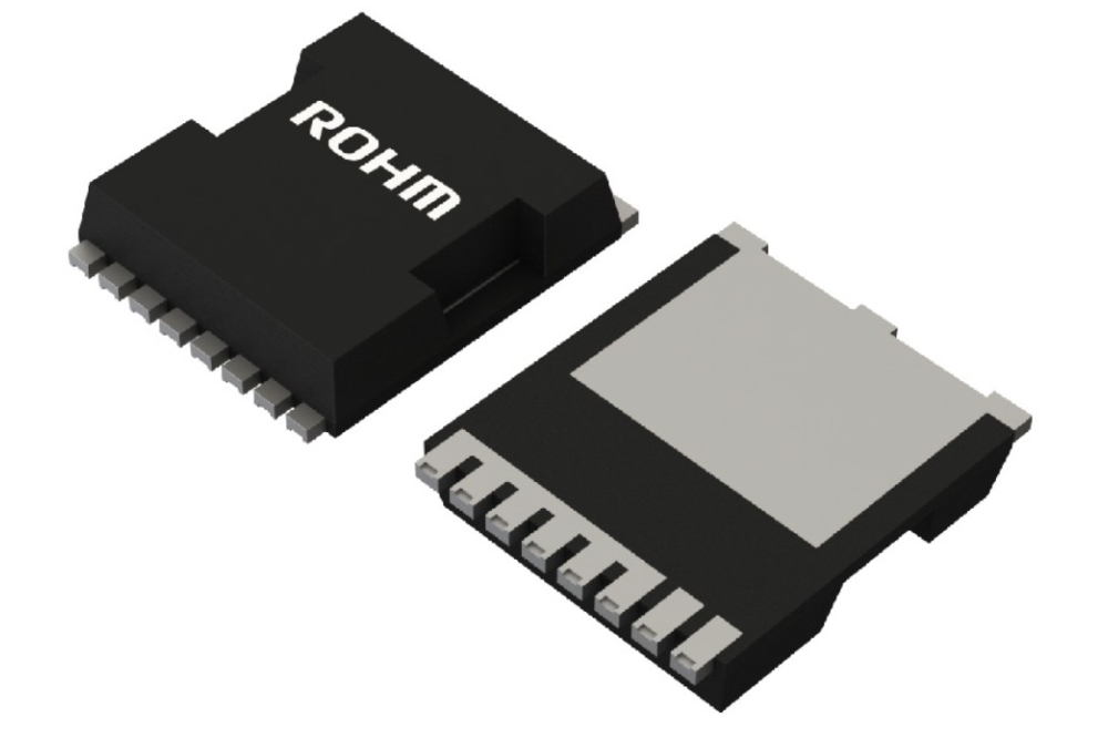
By 2010, two of the biggest hitters in the SiC industry, Cree (now Wolfspeed) and Rohm started to mass produce SiC MOSFETs. Which company won this race is a moot point to this day – both claim victory. The launch did not open the floodgates, with sales held back by high prices.
For example, not long after its launch, Cree’s MOSFET, sold through Digikey, retailed for $80 or more.
Since then prices have fallen, while the number of producers has expanded significantly. There is also more choice in blocking voltage and current handling, thanks to expanded portfolios and improved performance. All this activity is swelling sales, with many analysts claiming that global annual revenue for the SiC MOSFETs now exceeds $1 billion, and continues to climb at a very healthy rate.
A prize-winning bulb
2011. In the not-too-distant past, many of us would agonise over what to do when our lightbulb failed and we had to replace it. If trimming carbon footprints topped our agenda, we would select a compact fluorescent. But they were never a hit.
After installing one and flicking a switch, this bulb would take a minute or so to reach full brightness, by which time the room had been cast in a rather harsh light. Dimmer switches could not dial back the intensity, and when it came to disposal, care had to be taken with this mercury-ridden source.
If all those compromises were too much for us, we’d buy the well-established filament-based incandescent. It generated far more heat than light, and it didn’t last that long – 1,000 hours is typical – but it had many fans, as it instantly bathed the room with a lovely shade of white, and could be dimmed down.
Recognising these concerns and trying to do something about them, the US Department of Energy launched a competition in 2008 called the Bright Tomorrow Lighting Prize, better known as the L-Prize. $10 million were up for grabs, awarded to the first company that produced a bulb that combined the virtues of an incandescent with running costs that bettered a compact fluorescent and an incredibly long lifetime.
In August 2011 Philips claimed victory with a dimmable bulb that drew just 9.7 W while putting out a peak output of 910 lumens – that is 110 lumens more than a typical 60 W incandescent. Philips’ bulb underwent a range of tests to evaluate robustness, including being shaken, operated in temperature extremes and high levels of humidity, and driven with an imperfect voltage supply. Passing all evaluations with ease, it offered a lifetime of 25,000 hours, more than double that of a compact fluorescent.
When Philips launched this most impressive of sources it commanded a price so high that it would put off many early adopters. Would anyone really be willing to spend $50 on a single bulb?
Fortunately, prices have plummeted over the last few years. Today, if you shell out $50 on solid-state lighting, you could return from a hardware store with a score of Philips’ 60 W-equivalent LED bulbs. Thanks to these competitive prices, many homes are now lit by a collection of light-emitting chips.

The 60 W incandescent bulb has many great attributes: instant on, a nice warm hue, and the opportunity to dim output. The $10 million L-Prize challenged makers of LED bulbs to replicate all these merits, while drawing less than 10 W. Philips Lumileds got their first, before launching their award-winning bulb. One striking feature of this source is the yellow colour of its emitting surface, easily visible when the bulb is not on. The yellow is associated with the remote phosphor, which when pumped with a battalion of 18 LEDs, casts a room in uniform, warm shade of white light.
Gallium nitride gets its credentials
2012. Hero results pique interest but don’t guarantee sales. Designers want products that combine a great performance with longevity.
Developers at Transphorm understood this completely. They knew that their GaN FETs were attracting much attention, because they were a great product, exceeding the efficiency of silicon and coping far better at elevated temperatures. But to win sales, by assuring potential customers that they should not have any concerns over reliability, they put their 600V FET in for independent device testing. It passed, giving Transphorm, in 2012, the industry’s first GaN FET qualified to the JEDEC standard.
Initial products by this West-coast firm were produced on SiC substrates. But production soon switched to silicon. Merits of this move were not limited to a cheaper, larger foundation, but included the opportunity to process devices on mature 200 mm lines, potentially in under-utilised fabs.
More recently, Transphorm qualified its GaN-on-silicon FETs at standard temperatures and 175 °C. This helped to drive sales, which surpassed 500,000 in 2019. Fourth-generation products launched in 2020, taking performance of GaN-on-silicon FETs to a new high.
Last January Renesas announced that it would be acquiring Transphorm for $339 million. This deal went through in June, expanding the power portfolio of the Japanese chipmaker beyond silicon and SiC devices.

Droop’s smoking gun?
2013. Would it ever be possible to draw the debate on droop to a close? Given the competing, vigorously defended theories, it would require irrefutable proof. Obtaining this would not be easy, but in Spring 2013 claims of a smoking gun surfaced from a partnership between researchers at the University of California, Santa Barbara (UCSB), and the École Polytechnique in France.
This team’s evidence came from an extremely elegant experiment that drew parallels with that made by Robert Millikan at the start of the twentieth century. Millikan studied the photoelectric effect by measuring the kinetic energy of electrons exiting a metal bombarded with beams of photons.
On this more recent occasion researchers injected carriers into the quantum well and recorded two phenomena: the light emitted by the LED, and the energy of electrons exiting through the p-side of the device. To ensure all thermalised electrons left the LED, the p-side surface had been treated with caesium.
As the scientists from this collaboration cranked up the current through their device, they detected higher energy peaks, associated with the vacuum-emitted electrons. According to them, this observation provided unquestionable proof that Auger-Meitner is the cause of droop. In their view, no other mechanism could be responsible for these ‘hot’ electron peaks. Strengthening this claim, they found that when droop kicked in, high energy peaks started to emerge.
So, did other researchers working in this field raise a glass, toast this team’s success and agree that this work had put the debate on droop to bed? Absolutely not. In general, those that are trying to fathom the cause of droop have entrenched positions and are convinced that after examining all the evidence the theory they postulated is still the most convincing.
Critics argued that the experimental results may have been interpreted incorrectly. Boston University’s Enrico Bellotti claimed that the experiment suggests that electron leakage is the cause of droop, with some help from the Auger-Meitner effect.
Fred Schubert from Rensselaer Polytechnic Institute in Troy, NY, tended to agree, suggesting that some electrons detected in the experiment might not be associated with the Auger-Meitner effect at all, having simply leaked out of the LED’s quantum well. Another reason why Schubert struggles to view Auger-Meitner recombination as a major contributor to droop is that he considers droop to be stronger at low temperatures, while Auger is weaker.
The team from UCSB and the École Polytechnique addressed their critics in the November & December 2013 edition of Compound Semiconductor magazine. In their feature, they argued that in their LEDs, the electric field is not strong enough to cause electron leakage. They also countered claims that it would not be possible to observe Auger-Meitner-generated electrons escaping into vacuum, and expressed concerns related to a claim that free-carrier absorption could be a cause of droop.
Discussing competing theories will have helped to progress efforts to come to a consensus on the cause of droop. But even now, the debate has not completely disappeared.
By tracking the energy of non-radiative electrons that pass through an LED while simultaneously recording the light output of this device, researchers from the University of California, Santa Barbara, and the École Polytechnique, France, claimed they had definitive proof that the Auger-Meitner effect is the cause of droop.

In 2014, Infineon agreed to purchase International Rectifier for $3 billion. Orchestrators of the deal were Reinhard Ploss (left), CEO of Infineon Technologies, and Oleg Khaykin (right), President and CEO of International Rectifier.
A full complement
2014. The prospects of emerging devices can be judged by the actions of the biggest players manufacturing products with the incumbent technology. If alternatives have an outside chance of success, a few leading firms might dabble in them; and if they are certain to play a major role, multi-nationals will invest, either through acquisitions or internal development.
History now attests that the leading producers of power devices have made the right decision to invest heavily in wide bandgap technology. They have all branched out from considering only silicon devices, and made headway with either SiC or GaN, or both alternatives.
A trailblazer in diversification at scale is Infineon. It has not been hedging its bets as to which of these two rivals is going to play a bigger role, but has been pursuing both for more than a decade, viewing GaN as a strong candidate for below 600 V and SiC as the best option for higher voltages. A pioneer of commercialising SiC diodes and MOSFETs, Infineon did not embark on an internal development programme for GaN. Instead, it decided to acquire this technology. In 2014, it agreed to shell out $3 billion in cash for GaN-on-silicon pioneer International Rectifier (IR). Note, however, that as well as gaining IR’s GaN-based technology, it also picked up its low-voltage silicon MOSFET family, which accounted for the lion’s share of sales. When Infineon took IR into its fold, it viewed GaN-on-silicon as a long-term investment, generating sales at least five years down the line.
In March 2015, Infineon deepened its involvement in GaN, teaming up with Panasonic. This duo signed a deal committing them to jointly develop devices that combined Panasonic’s normally-off GaN-on-silicon transistors with Infineon’s surface-mounted packages that would house these chips.
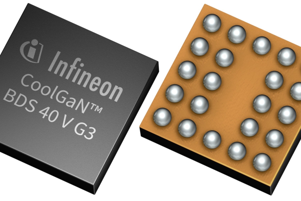
More recently, Infineon has broadened its portfolio of CoolGaN products, made using its own devices. So GaN is underway and SiC and silicon are well established, giving this German powerhouse an incredibly broad portfolio.

In 2014, Infineon agreed to purchase International Rectifier for $3 billion. Orchestrators of the deal were Reinhard Ploss (left), CEO of Infineon Technologies, and Oleg Khaykin (right), President and CEO of International Rectifier.