
Slashing the sheet resistance of ScAlN
A Chinese collaboration is claiming to have broken new ground in reducing the sheet resistance of ScAlN/GaN heterostructures grown on sapphire.
The success of the team – a partnership between researchers at Peking University, the Songshan Lake Materials Laboratory in Dongguan, and the Collaborative Innovation Centre of Quantum Matter, Beijing – attributes its low sheet resistance, just 137 W/sq, to employing an indium surfactant and introducing an ultrathin AlN interlayer.
According to the spokesperson for these researchers, Ping Wang from Peking University, their work addresses a critical bottleneck in the development of ScAlN-based high-frequency and high-power electronics – their breakthrough is the realisation of a high carrier density and high carrier mobility simultaneously on large-area, low-cost wafers.
Wang told Compound Semiconductor that the team’s work demonstrates a scalable route to integrating scandium-based semiconductors with mainstream GaN, silicon and CMOS technologies.
“Our findings will most directly benefit high-frequency and high-power GaN HEMTs, RF front-end modules, and microwave amplifiers, where low sheet resistance and high 2DEG mobility are essential for improving gain and power efficiency,” remarked Wang.
Additional strengths of the heterostructures produced by the Chinese collaboration are a sharp interface between ScAlN and GaN and excellent structural coherence. These traits are advantageous for ferroelectric transistors, non-volatile memories, and reconfigurable logic devices that exploit the strong polarisation and emerging ferroelectricity of ScAlN.
Researchers at Peking University have previously employed an indium surfactant for the growth of ScAlInN alloys and ScAlInN/GaN heterostructures.
“We observed that even trace indium incorporation during low-temperature growth could drastically improve interface quality, domain structure, and promote step-flow epitaxy,” explained Wang.
During that study, Wang and co-workers discovered that indium could act as a volatile surfactant for enhancing adatom diffusion of scandium and aluminium without being incorporated into the lattice.
The latest success is the culmination of a comprehensive investigation, involving the production of a wide portfolio of heterostructures, each including the ternary alloy ScAlN. All these samples were produced in a plasma-enhanced MBE system featuring Knudsen effusion cells for the supply of elemental gallium, aluminium and scandium. A Veeco RF plasma source provided active nitrogen species.
Wang and co-workers acquired atomic force microscopy maps of samples with a 20 nm-thick ScAlN layer with a scandium content ranging from 0.18 to 0.23. Scans revealed smooth morphologies and well-defined atomic steps. Increases in scandium content resulted in a change from GaN-like step-spiral features, indicative of step-flow growth, to a more metal-rich surface with clearer atomic surfaces, and eventually the emergence of island-like features.
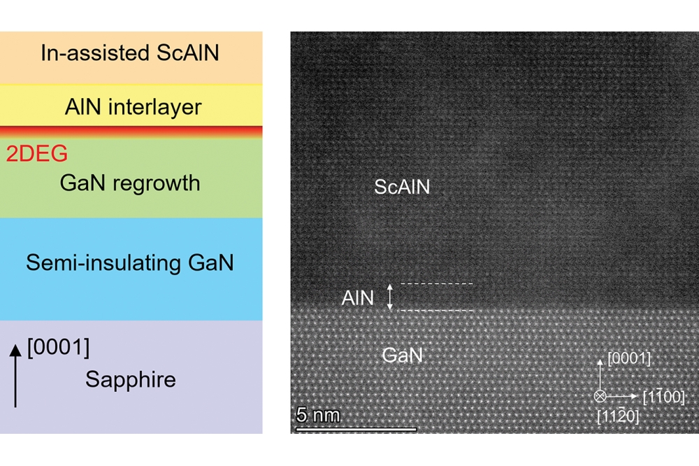
To build on their indium-surfactant-assisted growth, the team introduced an AlN interlayer between the ScAlN barrier and GaN channel to improve interfacial quality. It’s claimed that this interlayer supresses interface roughness scattering by promoting a more abrupt transition between ScAlN and GaN layers, and thereby enhancing electron mobility.
Electrical measurements on a range of samples with a ScAlN barrier just 10 nm-thick, trimmed to account for the influence of the AlN interlayer on electron mobility and sheet carrier density, revealed that the best results are realised with an AlN layer that’s 1 nm-thick and 10 nm-thick Sc0.21Al0.79N. For this structure, a sheet resistance of just 137 W/sq is realised alongside an electron mobility of 1020 cm2 V-1 s-1 and an electron sheet density of 4.5 x 1013 cm-2.
Wang explained that the team’s next step is to integrate their high-quality ScAlN heterostructures into functional prototypes, including HEMTs, ferroelectric FETs, and multi-state non-volatile memories.
Another goal is to explore polarisation-engineered ScAlN heterostructures and domain-wall-controlled ferroelectric devices. The latter could merge high-frequency performance with non-volatile programmability.
“In parallel, we are expanding the indium-assisted growth strategy to larger wafer formats and alternative ultrawide-bandgap substrates, such as SiC, Ga2O3, and diamond, aiming to bridge advanced ScAlN materials research with industrial-scale GaN electronics and future ultra-low-power intelligent systems,” added Wang.
Reference
L. Yang et al. Appl. Phys. Lett 127 152101 (2025)


